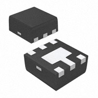
GMF05C-HS3
Vishay Semiconductors
5-Line ESD Protection Diode Array in LLP75-6A
Features
• Ultra compact LLP75-6A package
• 5-line ESD-protection
• Surge immunity acc.
IEC 61000-4-5 IPPM > 12 A
• Low leakage current IR < 1 µA
• ESD-immunity acc. IEC 61000-4-2
± 30 kV contact discharge
± 30 kV air discharge
• Working voltage range VRWM = 5 V
• Lead (Pb)-free component
• Component in accordance to RoHS 2002/95/EC
and WEEE 2002/96/EC
19957
6
5
4
1
2
3
1
19956
Marking (example only)
XX
YY
Dot = Pin 1 marking
XX = Date code
YY = Type code (see table below)
21001
Ordering Information
Ordering code
Taped units per reel
(8 mm tape on 7" reel)
Minimum order quantity
GMF05C-HS3-GS08
3000
15000
Device name
GMF05C-HS3
Package Data
Device name
GMF05C-HS3
Package
name
Type
code
Weight
Molding
compound
flammability rating
LLP75-6A
F5
5.2 mg
UL 94 V-0
Moisture sensitivity level
Soldering conditions
MSL level 1 (according J-STD-020) 260 °C/10 s at terminals
* Please see document “Vishay Green and Halogen-Free Definitions (5-2008)” http://www.vishay.com/doc?99902
Document Number 85654
Rev. 1.8, 23-Sep-08
For technical support, please contact: ESD-Protection@vishay.com
www.vishay.com
1
�GMF05C-HS3
Vishay Semiconductors
Absolute Maximum Ratings
Rating
Test condition
Symbol
Value
Unit
Peak pulse current
BiAs-mode: each input (pin 1; 3 - pin 6) to ground (pin 2);
acc. IEC 61000-4-5; tp = 8/20 µs; single shot
IPPM
12
A
Peak pulse power
BiAs-mode: each input (pin 1; 3 - pin 6) to ground (pin 2);
acc. IEC 61000-4-5; tp = 8/20 µs; single shot
PPP
200
W
contact
discharge
VESD
± 30
kV
air
discharge
VESD
± 30
kV
TJ
- 55 to + 125
°C
TSTG
- 55 to + 150
°C
ESD immunity
acc. IEC61000-4-2; 10 pulses
BiAs-mode: each input (pin 1; 3 - pin 6) to ground (pin 2)
Operating temperature
Junction temperature
Storage temperature
BiAs-Mode (5-line Bidirectional Asymmetrical protection mode)
With the GMF05C-HS3 up to 5 signal- or data-lines (L1 - L5) can be protected against voltage transients. With
pin 2 connected to ground and pin 1; 3 up tp pin 6 connected to a signal- or data-line which has to be protected.
As long as the voltage level on the data- or signal-line is between 0 V (ground level) and the specified Maximum
Reverse Working Voltage (VRWM) the protection diode between data line and ground offer a high isolation to
the ground line. The protection device behaves like an open switch.
As soon as any positive transient voltage signal exceeds the break through voltage level of the protection
diode, the diode becomes conductive and shorts the transient current to ground. Now the protection device
behaves like a closed switch. The Clamping Voltage (VC) is defined by the BReakthrough Voltage (VBR) level
plus the voltage drop at the series impedance (resistance and inductance) of the protection device.
Any negative transient signal will be clamped accordingly. The negative transient current is flowing in the
forward direction of the protection diode. The low Forward Voltage (VF) clamps the negative transient close to
the ground level.
Due to the different clamping levels in forward and reverse direction the GMF05C-HS3 clamping behaviour is
Bidirectional and Asymmetrical (BiAs).
L1
L2
1
5
2
4
3
3
L5
L4
L3
20739
www.vishay.com
2
For technical support, please contact: ESD-Protection@vishay.com
Document Number 85654
Rev. 1.8, 23-Sep-08
�GMF05C-HS3
Vishay Semiconductors
Electrical Characteristics
Ratings at 25 °C, ambient temperature unless otherwise specified
GMF05C-HS3
BiAs mode: each input (pin 1; 3 - pin 6) to ground (pin 2)
Parameter
Protection paths
Reverse working voltage
Reverse current
Reverse breakdown voltage
Test conditions/remarks
Symbol
Min.
Typ.
number of line which can be protected
N lines
at IR = 1 µA
VRWM
at VR = VRWM = 5 V
IR
at IR = 1 mA
VBR
at IPP = 12 A acc. IEC 61000-4-5
VC
at IPP = 1 A acc. IEC 61000-4-5
VC
at IF = 12 A acc. IEC 61000-4-5
VF
at IPP = 1 A acc. IEC 61000-4-5
VF
1.5
at VR = 0 V; f = 1 MHz
CD
126
at VR = 2.5 V; f = 1 MHz
CD
76
Max.
Unit
5
lines
5
V
< 0.1
6
1
µA
8
V
12.5
V
9.5
V
5.5
V
Reverse clamping voltage
7.8
Forward clamping voltage
V
150
pF
Capacitance
pF
If a higher surge current or Peak Pulse current (IPP) is needed, some protection diodes in the GMF05C-HS3
can also be used in parallel in order to "multiply" the performance.
If two diodes are switched in parallel you get
•
double surge power = double peak pulse current (2 x IPPM)
•
half of the line inductance = reduced clamping voltage
•
half of the line resistance = reduced clamping voltage
•
double line Capacitance (2 x CD)
•
double Reverse leakage current (2 x IR)
L1
1
6
2
5
3
4
L2
L3
20740
Document Number 85654
Rev. 1.8, 23-Sep-08
For technical support, please contact: ESD-Protection@vishay.com
www.vishay.com
3
�GMF05C-HS3
Vishay Semiconductors
Typical Characteristics
Tamb = 25 °C, unless otherwise specified
100
120 %
BiAs-mode
Rise time = 0.7 ns to 1 ns
Discharge Current IESD
100 %
10
80 %
IF (mA)
1
60 %
53 %
0.1
40 %
27 %
0.01
20 %
0.001
0.5
0%
- 10 0 10 20 30 40 50 60 70 80 90 100
0.6
0.7
Figure 1. ESD Discharge Current Wave Form
acc. IEC 61000-4-2 (330 Ω/150 pF)
0.8
0.9
VF (V)
21205
Time (ns)
20557
Figure 4. Typical Forward Current IF vs. Forward Voltage VF
7
8 µs to 100 %
100 %
6
80 %
5
20 µs to 50 %
BiAs-mode
4
VR (V)
IPPM
60 %
3
40 %
2
20 %
1
0
0.01
0%
0
10
20
20548
30
40
Time (µs)
0.1
1
10
1000 10000
IR (µA)
21206
Figure 2. 8/20 µs Peak Pulse Current Wave Form
(acc. IEC 61000-4-5)
100
Figure 5. Typical Reverse Voltage VR vs.
Reverse Current IR
140
14
f = 1 MHz
120
BiAs-mode
10
80
VC (V)
CD (pF)
100
60
8
6
40
4
20
2
0
0
21204
1
2
3
4
5
VR (V)
www.vishay.com
Measured
acc. IEC 61000-4-5
(8/20 µs - wave form)
VC
0
6
Figure 3. Typical Capacitance CD vs. Reverse Voltage VR
4
BiAs-mode
12
0
2
4
21207
6
8
10
12
14
16
IPP (A)
Figure 6. Typical Peak Clamping Voltage VC vs.
Peak Pulse Current IPP
For technical support, please contact: ESD-Protection@vishay.com
Document Number 85654
Rev. 1.8, 23-Sep-08
�GMF05C-HS3
Vishay Semiconductors
80
acc. IEC 61000-4-2
+ 8 kV
contact discharge
60
VC-ESD (V)
40
20
0
- 20
- 40
- 60
- 10 0
10 20 30 40 50 60 70 80 90
21208
t (ns)
Figure 7. Typical Clamping Performance at + 8 kV
Contact Discharge (acc. IEC 61000-4-2)
60
acc. IEC 61000-4-2
- 8 kV
contact discharge
40
VC-ESD (V)
20
0
- 20
- 40
- 60
- 80
- 10 0 10 20 30 40 50 60 70 80 90
t (ns)
21209
Figure 8. Typical Clamping Performance at - 8 kV
Contact Discharge (acc. IEC 61000-4-2)
250
200
150
negative
discharge
VC-ESD (V)
100
50
VC-ESD
0
- 50
positive
- 100 discharge
- 150
acc. IEC 61000-4-2
- 200
contact discharge
- 250
0
5
10
15
21210
20
25
30
VESD (kV)
Figure 9. Typical Peak Clamping Voltage at ESD
Contact Discharge (acc. IEC 61000-4-2)
Document Number 85654
Rev. 1.8, 23-Sep-08
For technical support, please contact: ESD-Protection@vishay.com
www.vishay.com
5
�GMF05C-HS3
Vishay Semiconductors
Package Dimensions in millimeters (inches): LLP75-6A
18058
www.vishay.com
6
For technical support, please contact: ESD-Protection@vishay.com
Document Number 85654
Rev. 1.8, 23-Sep-08
�GMF05C-HS3
Vishay Semiconductors
Ozone Depleting Substances Policy Statement
It is the policy of Vishay Semiconductor GmbH to
1. Meet all present and future national and international statutory requirements.
2. Regularly and continuously improve the performance of our products, processes, distribution and operating
systems with respect to their impact on the health and safety of our employees and the public, as well as
their impact on the environment.
It is particular concern to control or eliminate releases of those substances into the atmosphere which are
known as ozone depleting substances (ODSs).
The Montreal Protocol (1987) and its London Amendments (1990) intend to severely restrict the use of ODSs
and forbid their use within the next ten years. Various national and international initiatives are pressing for an
earlier ban on these substances.
Vishay Semiconductor GmbH has been able to use its policy of continuous improvements to eliminate the use
of ODSs listed in the following documents.
1. Annex A, B and list of transitional substances of the Montreal Protocol and the London Amendments
respectively.
2. Class I and II ozone depleting substances in the Clean Air Act Amendments of 1990 by the Environmental
Protection Agency (EPA) in the USA.
3. Council Decision 88/540/EEC and 91/690/EEC Annex A, B and C (transitional substances) respectively.
Vishay Semiconductor GmbH can certify that our semiconductors are not manufactured with ozone depleting
substances and do not contain such substances.
We reserve the right to make changes to improve technical design
and may do so without further notice.
Parameters can vary in different applications. All operating parameters must be validated for each customer
application by the customer. Should the buyer use Vishay Semiconductors products for any unintended or
unauthorized application, the buyer shall indemnify Vishay Semiconductors against all claims, costs, damages,
and expenses, arising out of, directly or indirectly, any claim of personal damage, injury or death associated
with such unintended or unauthorized use.
Vishay Semiconductor GmbH, P.O.B. 3535, D-74025 Heilbronn, Germany
Document Number 85654
Rev. 1.8, 23-Sep-08
For technical support, please contact: ESD-Protection@vishay.com
www.vishay.com
7
�LLP75-6A
Vishay Semiconductors
LLP75-6A
Package Dimensions in mm (Inches)
18058
Document Number 84020
Rev. 1.2, 07-Dec-06
www.vishay.com
1
�LLP75-6A
Vishay Semiconductors
LLP75-6A
Package Dimensions in mm (Inches)
18058
Document Number 84020
Rev. 1.2, 07-Dec-06
www.vishay.com
1
�LLP75-6A
Vishay Semiconductors
Ozone Depleting Substances Policy Statement
It is the policy of Vishay Semiconductor GmbH to
1. Meet all present and future national and international statutory requirements.
2. Regularly and continuously improve the performance of our products, processes, distribution and operating
systems with respect to their impact on the health and safety of our employees and the public, as well as
their impact on the environment.
It is particular concern to control or eliminate releases of those substances into the atmosphere which are
known as ozone depleting substances (ODSs).
The Montreal Protocol (1987) and its London Amendments (1990) intend to severely restrict the use of ODSs
and forbid their use within the next ten years. Various national and international initiatives are pressing for an
earlier ban on these substances.
Vishay Semiconductor GmbH has been able to use its policy of continuous improvements to eliminate the use
of ODSs listed in the following documents.
1. Annex A, B and list of transitional substances of the Montreal Protocol and the London Amendments
respectively
2. Class I and II ozone depleting substances in the Clean Air Act Amendments of 1990 by the Environmental
Protection Agency (EPA) in the USA
3. Council Decision 88/540/EEC and 91/690/EEC Annex A, B and C (transitional substances) respectively.
Vishay Semiconductor GmbH can certify that our semiconductors are not manufactured with ozone depleting
substances and do not contain such substances.
We reserve the right to make changes to improve technical design
and may do so without further notice.
Parameters can vary in different applications. All operating parameters must be validated for each
customer application by the customer. Should the buyer use Vishay Semiconductors products for any
unintended or unauthorized application, the buyer shall indemnify Vishay Semiconductors against all
claims, costs, damages, and expenses, arising out of, directly or indirectly, any claim of personal
damage, injury or death associated with such unintended or unauthorized use.
Vishay Semiconductor GmbH, P.O.B. 3535, D-74025 Heilbronn, Germany
www.vishay.com
2
Document Number 84020
Rev. 1.2, 07-Dec-06
�Legal Disclaimer Notice
www.vishay.com
Vishay
Disclaimer
ALL PRODUCT, PRODUCT SPECIFICATIONS AND DATA ARE SUBJECT TO CHANGE WITHOUT NOTICE TO IMPROVE
RELIABILITY, FUNCTION OR DESIGN OR OTHERWISE.
Vishay Intertechnology, Inc., its affiliates, agents, and employees, and all persons acting on its or their behalf (collectively,
“Vishay”), disclaim any and all liability for any errors, inaccuracies or incompleteness contained in any datasheet or in any other
disclosure relating to any product.
Vishay makes no warranty, representation or guarantee regarding the suitability of the products for any particular purpose or
the continuing production of any product. To the maximum extent permitted by applicable law, Vishay disclaims (i) any and all
liability arising out of the application or use of any product, (ii) any and all liability, including without limitation special,
consequential or incidental damages, and (iii) any and all implied warranties, including warranties of fitness for particular
purpose, non-infringement and merchantability.
Statements regarding the suitability of products for certain types of applications are based on Vishay’s knowledge of typical
requirements that are often placed on Vishay products in generic applications. Such statements are not binding statements
about the suitability of products for a particular application. It is the customer’s responsibility to validate that a particular
product with the properties described in the product specification is suitable for use in a particular application. Parameters
provided in datasheets and/or specifications may vary in different applications and performance may vary over time. All
operating parameters, including typical parameters, must be validated for each customer application by the customer’s
technical experts. Product specifications do not expand or otherwise modify Vishay’s terms and conditions of purchase,
including but not limited to the warranty expressed therein.
Except as expressly indicated in writing, Vishay products are not designed for use in medical, life-saving, or life-sustaining
applications or for any other application in which the failure of the Vishay product could result in personal injury or death.
Customers using or selling Vishay products not expressly indicated for use in such applications do so at their own risk and agree
to fully indemnify and hold Vishay and its distributors harmless from and against any and all claims, liabilities, expenses and
damages arising or resulting in connection with such use or sale, including attorneys fees, even if such claim alleges that Vishay
or its distributor was negligent regarding the design or manufacture of the part. Please contact authorized Vishay personnel to
obtain written terms and conditions regarding products designed for such applications.
No license, express or implied, by estoppel or otherwise, to any intellectual property rights is granted by this document or by
any conduct of Vishay. Product names and markings noted herein may be trademarks of their respective owners.
Material Category Policy
Vishay Intertechnology, Inc. hereby certifies that all its products that are identified as RoHS-Compliant fulfill the
definitions and restrictions defined under Directive 2011/65/EU of The European Parliament and of the Council
of June 8, 2011 on the restriction of the use of certain hazardous substances in electrical and electronic equipment
(EEE) - recast, unless otherwise specified as non-compliant.
Please note that some Vishay documentation may still make reference to RoHS Directive 2002/95/EC. We confirm that
all the products identified as being compliant to Directive 2002/95/EC conform to Directive 2011/65/EU.
Revision: 12-Mar-12
1
Document Number: 91000
�