Bulletin PD-20618 rev. D 10/06
HFA08SD60S
Ultrafast, Soft Recovery Diode
Features
t rr = 18ns
IF(AV) = 8Amp
VR = 600V
Ultrafast Recovery Time
Ultrasoft Recovery
Very Low IRRM
Very Low Qrr
Guaranteed Avalanche
Specified at Operating Temperature
Benefits
Reduced RFI and EMI
Reduced Power Loss in Diode and
Switching Transistor
Higher Frequency Operation
Reduced Snubbing
Reduced Parts Count
Description/ Applications
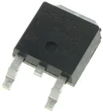
Package Outline
These diodes are optimized to reduce losses and EMI/RFI in
high frequency power conditioning systems. The softness of
the recovery eliminates the need for a snubber in most
applications. These devices are ideally suited for freewheeling,
flyback, power converters, motor drives, and other applications
where high speed and reduced switching losses are design
requirements.
D - PAK
Absolute Maximum Ratings
Parameters
VRRM
Cathode-to-Anode Voltage
IF(AV)
Continuous Forward Current
Max
Units
600
V
8
A
TC = 100°C
IFSM
Single Pulse Forward Current
60
IFRM
Peak Repetitive Forward Current
24
PD
Maximum Power Dissipation
14
W
- 55 to 150
°C
TC = 100°C
TJ, TSTG
Operating Junction and Storage Temperatures
Document Number: 93039
www.vishay.com
1
�HFA08SD60S
Bulletin PD-20618 rev. D 10/06
Electrical Characteristics @ TJ = 25°C (unless otherwise specified)
Parameters
Min Typ Max Units Test Conditions
VBR, Vr
Breakdown Voltage,
Blocking Voltage
600
-
-
V
IR = 100µA
VF
Forward Voltage
-
1.4
1.7
V
IF = 8A
See Fig. 1
-
1.7
2.1
V
IF = 16A
-
1.4
1.7
V
IF = 8A, TJ = 125°C
-
0.3
5.0
µA
VR = VR Rated
-
100
500
µA
TJ = 125°C, VR = 0.8 x VR Rated
IR
Max. Reverse Leakage Current
CT
Junction Capacitance
-
10
25
pF
VR = 200V
LS
Series Inductance
-
8.0
-
nH
Measured lead to lead 5mm from package body
Dynamic Recovery Characteristics @ TJ = 25°C (unless otherwise specified)
Parameters
trr
Reverse Recovery Time
IRRM
Qrr
Peak Recovery Current
Reverse Recovery Charge
di(rec)M/dt Rate of Fall of recovery Current
Min Typ Max Units Test Conditions
-
18
-
-
37
55
TJ = 25°C
IF = 8A
-
55
90
TJ = 125°C
-
3.5
5.0
VR = 200V
diF /dt = 200A/µs
-
4.5
8.0
-
65
138
-
124
360
-
240
-
-
210
-
ns
A
IF = 1.0A, diF/dt = 200A/µA, VR = 30V
TJ = 25°C
TJ = 125°C
nC
TJ = 25°C
TJ = 125°C
A/µs
TJ = 25°C
TJ = 125°C
Thermal - Mechanical Characteristics
Parameters
Min
Typ
Max
Units
TJ
Max. Junction Temperature Range
-
-
- 55 to 150
TStg
Max. Storage Temperature Range
-
-
- 55 to 150
Tlead
Lead Temperature
-
-
300
RthJC
Thermal Resistance, Junction to Case
-
-
3.5
RthJA
Thermal Resistance, Junction to Ambient
-
-
80
Wt
Weight
-
2.0
-
g
-
0.07
-
(oz)
°C
°C/ W
Typical Socket Mount
Document Number: 93039
www.vishay.com
2
�HFA08SD60S
Bulletin PD-20618 rev. D 10/06
100
1000
(µA)
100
Reverse Current - I
(A)
R
125˚C
10
1
25˚C
0.1
0.01
0.001
0
100
200
300
400
500
600
Reverse Voltage - V R (V)
Fig. 2 - Typical Values Of Reverse Current
Vs. Reverse Voltage
100
Junction Capacitance - C T (pF)
Instantaneous Forward Current - I
F
10
T J = 150˚C
1
T = 150˚C
J
T = 125˚C
J
T = 25˚C
J
0.1
0.4 0.8 1.2 1.6
2
2.4 2.8 3.2 3.6
T J = 25˚C
10
1
4
Forward Voltage Drop - V FM (V)
1
10
100
1000
Reverse Voltage - V R (V)
Fig. 3 - Typical Junction Capacitance
Vs. Reverse Voltage
Fig. 1 - Typical Forward Voltage Drop Characteristics
Thermal Impedance Z
thJC
(°C/W)
10
1
D = 0.50
D = 0.20
D = 0.10
D = 0.05
D = 0.02
D = 0.01
0.1
0.01
0.00001
Document Number: 93039
PDM
t1
Single Pulse
(Thermal Resistance)
0.0001
0.001
t2
Notes:
1. Duty factor D = t1/ t2
2. Peak Tj = Pdm x ZthJC + Tc
0.01
0.1
t1, Rectangular Pulse Duration (Seconds)
Fig. 4 - Max. Thermal Impedance Z thJC Characteristics
1
www.vishay.com
3
�HFA08SD60S
Bulletin PD-20618 rev. D 10/06
20
80
If = 16A
If = 8A
If = 4A
70
Irr (A)
trr (ns)
50
40
30
20
10
5
Vr = 200V
Tj = 125˚C
Tj = 25˚C
Vr = 200V
Tj = 125˚C
Tj = 25˚C
10
100
0
100
1000
diF /dt (A/ µs)
Vr = 200V
Tj = 125˚C
Tj = 25˚C
Vr = 200V
Tj = 125˚C
Tj = 25˚C
If = 16A
If = 8A
If = 4A
di (rec)M / dt (A/ µs)
Qrr ( nC )
Fig. 6 - Typical Recovery Current vs. di F /dt
10000
500
300
1000
Average Forward Current - IF(AV) (A)
Fig. 5 - Typical Reverse Recovery vs. di F /dt
400
If = 16A
If = 8A
If = 4A
15
60
200
If = 16A
If = 8A
If = 4A
1000
100
0
100
1000
di F /dt (A/µs )
Fig. 7 - Typical Stored Charge vs. di F /dt
Document Number: 93039
100
100
1000
di F /dt (A/µs )
Fig. 8 - Typical di (rec)M /dt vs. di F /dt
www.vishay.com
4
�HFA08SD60S
Bulletin PD-20618 rev. D 10/06
Reverse Recovery Circuit
VR = 200V
0.01 Ω
L = 70µH
D.U.T.
D
di F /dt
dif/dt
ADJUST G
IRFP250
S
Fig. 9- Reverse Recovery Parameter Test Circuit
3
t rr
IF
tb
ta
0
2
Q rr
I RRM
4
0.5 I RRM
di(rec)M/dt
5
0.75 I RRM
1
di fF/dt
/dt
1. diF /dt - Rate of change of current through zero
crossing
2. IRRM - Peak reverse recovery current
3. trr - Reverse recovery time measured from zero
crossing point of negative going IF to point where
a line passing through 0.75 IRRM and 0.50 IRRM
extrapolated to zero current
4. Qrr - Area under curve defined by t rr
and IRRM
t rr x I RRM
Q rr =
2
5. di (rec)M /dt - Peak rate of change of
current during t b portion of t rr
Fig. 10 - Reverse Recovery Waveform and Definitions
Document Number: 93039
www.vishay.com
5
�HFA08SD60S
Bulletin PD-20618 rev. D 10/06
Outline Table
2.38 (0.09)
6.73 (0.26)
2.19 (0.08)
1.14 (0.04)
6.35 (0.25)
MINIMUM RECOMMENDED FOOTPRINT
0.89 (0.03)
5.46 (0.21)
1.27 (0.05)
5.21 (0.20)
0.58 (0.02)
0.88 (0.03)
0.46 (0.02)
5.97 (0.24)
4
6.45 (0.24)
6.22 (0.24)
1.64 (0.02)
5.68 (0.22)
5.97 (0.23)
1
2
6.48 (0.26)
10.42 (0.41)
10.67 (0.42)
9.40 (0.37)
3
0.51 (0.02)
MIN.
1.52 (0.06)
2x
2.54 (0.10)
1.15 (0.04)
2x
3x
1.14 (0.04)
0.76 (0.03)
0.89 (0.03)
0.64 (0.02)
0.58 (0.02)
1.65 (0.06)
0.46 (0.02)
2x
2.28 (0.09)
2x
2
1 - Anode
2.28 (0.09)
2x
12 -- NC
Cathode
Anode
23 -- Cathode
4 - Cathode
3 - Anode
4 - Cathode
4.57 (0.18)
Conform to JEDEC outline D-Pak
Dimensions in millimeters and (inches)
3
1
Anode
N/C
Tape & Reel Information
TRR
1.60 (0.063)
1.50 (0.059)
4.10 (0.161)
3.90 (0.153)
1.60 (0.063)
1.50 (0.059)
DIA.
0.368 (0.0145)
0.342 (0.0135)
FEED DIRECTION
1.85 (0 .07 3)
1.65 (0 .06 5)
11.60 (0.457)
11.40 (0.449)
15 .42 (0.6 09)
15 .22 (0.6 01)
TRL
1.75 (0.06 9)
10 .90 (0.4 29)
10 .70 (0.4 21)
1.25 (0.04 9)
24 .30 (0 .95 7)
23 .90 (0 .94 1)
DIA.
16 .10 (0.6 34)
4.72 (0.186)
4.52 (0.178)
15 .90 (0.6 26)
FEED DIRECTION
13.50 (0.532)
12.80 (0.504) DIA.
26 .40 (1.0 39)
24 .40 (0.9 61)
SMD-220 Tape & Reel
When ordering, indicate the part
360 (14.173)
DIA. MAX.
Document Number: 93039
60 (2 .36 2)
D IA . MIN .
Tape
number,SMD-220
part orientation,
and &
theReel
quantity.
Quantities
are in multiples
When
ordering,
indicate the part
of 800 pieces per reel for both
number, part orientation and the
TRL and TRR.
quantity. Quantities are in
multiples of 800 pieces per reel
for both TRL and TRR.
www.vishay.com
6
�HFA08SD60S
Bulletin PD-20618 rev. D 10/06
Marking Information
2 (K)
INTERNATIONAL
EXAMPLE: THIS IS AN HFA08SD60S
RECTIFIER LOGO
PART NUMBER
HFA08SD60S
9812
5K3A
ASSEMBLY
DATE CODE (YYWW)
LOT CODE
NC
3 (A)
YY = YEAR
WW = WEEK
Ordering Information Table
Device Code
HF
A
08
SD
60
S
1
2
3
4
5
6
1
-
Hexfred Family
2
-
Electron Irradiated
3
-
Current Rating (08 = 8A)
4
-
D-PAK
5
-
Voltage Rating (60 = 600V)
6
-
Suffix
S
= D2PAK/ Dpak
TR = Tape & Reel
TRL = Tape & Reel Left
TRR= Tape & Reel Right
Data and specifications subject to change without notice.
This product has been designed and qualified for Industrial Level.
Qualification Standards can be found on IR's Web site.
IR WORLD HEADQUARTERS: 233 Kansas St., El Segundo, California 90245, USA Tel: (310) 252-7105
TAC Fax: (310) 252-7309
10/2006
Document Number: 93039
www.vishay.com
7
�Legal Disclaimer Notice
Vishay
Notice
The products described herein were acquired by Vishay Intertechnology, Inc., as part of its acquisition of
International Rectifier’s Power Control Systems (PCS) business, which closed in April 2007. Specifications of the
products displayed herein are pending review by Vishay and are subject to the terms and conditions shown below.
Specifications of the products displayed herein are subject to change without notice. Vishay Intertechnology, Inc., or
anyone on its behalf, assumes no responsibility or liability for any errors or inaccuracies.
Information contained herein is intended to provide a product description only. No license, express or implied, by
estoppel or otherwise, to any intellectual property rights is granted by this document. Except as provided in Vishay's
terms and conditions of sale for such products, Vishay assumes no liability whatsoever, and disclaims any express
or implied warranty, relating to sale and/or use of Vishay products including liability or warranties relating to fitness
for a particular purpose, merchantability, or infringement of any patent, copyright, or other intellectual property right.
The products shown herein are not designed for use in medical, life-saving, or life-sustaining applications.
Customers using or selling these products for use in such applications do so at their own risk and agree to fully
indemnify Vishay for any damages resulting from such improper use or sale.
International Rectifier®, IR®, the IR logo, HEXFET®, HEXSense®, HEXDIP®, DOL®, INTERO®, and POWIRTRAIN®
are registered trademarks of International Rectifier Corporation in the U.S. and other countries. All other product
names noted herein may be trademarks of their respective owners.
Document Number: 99901
Revision: 12-Mar-07
www.vishay.com
1
�