IL211AT, IL212AT, IL213AT
www.vishay.com
Vishay Semiconductors
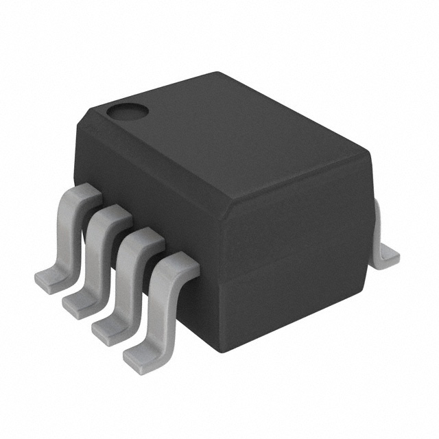
Optocoupler, Phototransistor Output,
with Base Connection in SOIC-8 Package
FEATURES
A 1
8
NC
• Isolation test voltage, 4000 VRMS
K 2
7
B
NC 3
6
C
• Industry standard SOIC-8 surface mountable
package
NC 4
5
E
• Compatible with dual wave, vapor phase and IR
reflow soldering
i179002-1
V
D E
i179025
• Material categorization:
for definitions of compliance please see
www.vishay.com/doc?99912
DESCRIPTION
The IL211AT, IL212AT, IL213AT are optically coupled pairs
with a gallium arsenide infrared LED and silicon NPN
phototransistor. Signal information, including a DC level,
can be transmitted by the device while maintaining a high
degree of electrical isolation between input and output.
AGENCY APPROVALS
The IL211AT, IL212AT, IL213AT comes in a standard
SOIC-8 small outline package for surface mounting which
makes it ideally suited for high density applications with
limited space. In addition to eliminating through-holes
requirements, this package conforms to standards for
surface mounted devices.
• DIN EN 60747-5-5 (pending) (1)
• UL1577, file no. E52744 system code Y
• cUL - file no. E52744, equivalent to CSA bulletin 5A
• DIN EN 60747-5-2 (VDE 0884) (1)
Note
(1) Available upon request, as option 1
A choice of 20 %, 50 %, and 100 % minimum CTR at
IF = 10 mA makes these optocouplers suitable for a variety
of different applications.
ORDERING INFORMATION
SOIC-8
I
L
2
1
#
A
T
6.1 mm
PART NUMBER
CTR (%)
AGENCY CERTIFIED/PACKAGE
10 mA
UL, cUL
> 20
> 50
> 100
SOIC-8
IL211AT
IL212AT
IL213AT
ABSOLUTE MAXIMUM RATINGS (Tamb = 25 °C, unless otherwise specified)
PARAMETER
TEST CONDITION
SYMBOL
VALUE
UNIT
INPUT
Peak reverse voltage
VR
6
V
Forward continuous current
IF
60
mA
Power dissipation
Pdiss
Derate linearly from 25 °C
90
mW
1.2
mW/°C
30
V
V
OUTPUT
Collector emitter breakdown voltage
BVCEO
Emitter collector breakdown voltage
BVECO
7
VCBO
70
V
ICMAX. DC
50
mA
ICMAX.
100
mA
Pdiss
150
mW
2
mW/°C
Collector base breakdown voltage
ICMAX. DC
ICMAX.
Power dissipation
Derate linearly from 25 °C
t < 1 ms
Document Number: 83615
1
For technical questions, contact: optocoupleranswers@vishay.com
THIS DOCUMENT IS SUBJECT TO CHANGE WITHOUT NOTICE. THE PRODUCTS DESCRIBED HEREIN AND THIS DOCUMENT
ARE SUBJECT TO SPECIFIC DISCLAIMERS, SET FORTH AT www.vishay.com/doc?91000
Rev. 1.9, 21-Dec-10
�IL211AT, IL212AT, IL213AT
www.vishay.com
Vishay Semiconductors
ABSOLUTE MAXIMUM RATINGS (Tamb = 25 °C, unless otherwise specified)
PARAMETER
TEST CONDITION
SYMBOL
VALUE
UNIT
VISO
4000
VRMS
Ptot
240
mW
3.2
mW/°C
Tstg
-55 to +150
°C
Tamb
-55 to +100
°C
10
s
COUPLER
Isolation test voltage
Total package dissipation
LED and detector
Derate linearly from 25 °C
Storage temperature
Operating temperature
Soldering time
at 260 °C
Note
• Stresses in excess of the absolute maximum ratings can cause permanent damage to the device. Functional operation of the device is not
implied at these or any other conditions in excess of those given in the operational sections of this document. Exposure to absolute
maximum ratings for extended periods of the time can adversely affect reliability.
ELECTRICAL CHARACTERISTICS (Tamb = 25 °C, unless otherwise specified)
PARAMETER
TEST CONDITION
PART
SYMBOL
MIN.
TYP.
MAX.
UNIT
INPUT
Forward voltage
IF = 10 mA
VF
-
1.3
1.5
V
Reverse current
VR = 6 V
IR
-
0.1
100
μA
Capacitance
VR = 0 V
CO
-
13
-
pF
OUTPUT
Collector emitter breakdown voltage
IC = 10 μA
BVCEO
30
-
-
V
Emitter collector breakdown voltage
IE = 10 μA
BVECO
7
-
-
V
Collector dark current
VCE = 10 V
ICEO
-
5
50
nA
Collector emitter capacitance
VCE = 0 V
CCE
-
10
IF = 10 mA
VCEsat
-
-
0.4
V
1s
VISO
4000
-
-
VRMS
CIO
-
0.5
50
pF
RIO
-
100
-
GΩ
BVCEO
30
-
-
V
pF
COUPLER
Saturation voltage, collector emitter
Isolation test voltage
Capacitance (input to output)
Resistance (input to output)
Collector emitter breakdown voltage
IC = 10 μA
Note
• Minimum and maximum values were tested requirements. Typical values are characteristics of the device and are the result of engineering
evaluations. Typical values are for information only and are not part of the testing requirements.
CURRENT TRANSFER RATIO
PARAMETER
Current transfer ratio
TEST CONDITION
IF = 10 mA, VCE = 5 V
PART
SYMBOL
MIN.
TYP.
MAX.
UNIT
IL211AT
CTR
20
50
-
%
IL212AT
CTR
50
80
-
%
IL213AT
CTR
100
130
-
%
PART
SYMBOL
MIN.
TYP.
MAX.
UNIT
ton, toff
-
3
-
μs
SWITCHING CHARACTERISTICS
PARAMETER
TEST CONDITION
Switching time
IC = 2 mA, RL = 100 Ω,
VCC = 10 V
Document Number: 83615
2
For technical questions, contact: optocoupleranswers@vishay.com
THIS DOCUMENT IS SUBJECT TO CHANGE WITHOUT NOTICE. THE PRODUCTS DESCRIBED HEREIN AND THIS DOCUMENT
ARE SUBJECT TO SPECIFIC DISCLAIMERS, SET FORTH AT www.vishay.com/doc?91000
Rev. 1.9, 21-Dec-10
�IL211AT, IL212AT, IL213AT
www.vishay.com
Vishay Semiconductors
SAFETY AND INSULATION RATINGS
PARAMETER
TEST CONDITION
Climatic classification
SYMBOL
MIN.
TYP.
MAX.
-
55 / 100 / 21
399
According to IEC 68 part 1
Comparative tracking index
CTI
UNIT
175
-
VIOTM
6000
-
-
V
VIORM
560
-
-
V
PSO
-
-
350
mW
ISI
-
-
150
mA
TSI
-
-
165
°C
Creepage distance
4
-
-
mm
Clearance distance
4
-
-
mm
Insulation thickness
0.2
-
-
mm
Note
• As per IEC 60747-5-2, § 7.4.3.8.1, this optocoupler is suitable for “Safe Electrical Insulation” only within the safety ratings. Compliance with
the safety ratings shall be ensured by means of protective circuits.
TYPICAL CHARACTERISTICS (Tamb = 25 °C, unless otherwise specified)
10 000
ICE0 - Leakage Current (nA)
VF - Forward Voltage (V)
1.8
1.6
Tamb = 0 °C
Tamb = - 40 °C
1.4
Tamb = - 55 °C
1.2
Tamb = 25 °C
Tamb = 50 °C
Tamb = 75 °C
1.0
0.8
Tamb = 100 °C
0.6
0.1
1
10
100
IF - Forward Current (mA)
22462
IF = 0 mA
1000
100
VCE = 12 V
0.1
0.01
0.001
- 60 - 40 - 20
0
20
40
60
80 100
Tamb - Ambient Temperature (°C)
Fig. 3 - Leakage Current vs. Ambient Temperature
50
30
45
IF = 30 mA
40
IC - Collector Current (mA)
IC - Collector Current (mA)
VCE = 24 V
1
22466
Fig. 1 - Forward Voltage vs. Forward Current
IF = 20 mA
35
30
IF = 15 mA
25
IF = 10 mA
20
15
IF = 5 mA
10
5
25
IF = 25 mA
20
IF = 10 mA
15
10
0
IF = 5 mA
5
IF = 1 mA
IF = 2 mA
0
0
22463
VCE = 40 V
10
1
2
3
4
5
6
7
8
VCE - Collector Emitter Voltage (NS) (V)
Fig. 2 - Collector Current vs. Collector Emitter Voltage
(non-saturated)
0
22464
0.1
0.2
0.3
0.4
VCE - Collector Emitter Voltage (sat) (V)
Fig. 4 - Collector Current vs. Collector Emitter Voltage
(saturated)
Document Number: 83615
3
For technical questions, contact: optocoupleranswers@vishay.com
THIS DOCUMENT IS SUBJECT TO CHANGE WITHOUT NOTICE. THE PRODUCTS DESCRIBED HEREIN AND THIS DOCUMENT
ARE SUBJECT TO SPECIFIC DISCLAIMERS, SET FORTH AT www.vishay.com/doc?91000
Rev. 1.9, 21-Dec-10
�IL211AT, IL212AT, IL213AT
www.vishay.com
Vishay Semiconductors
1.2
1.4
NCTR - Normalized CTR (NS)
NCTR - Normalized CTR (sat)
VCE = 5 V
IF = 10 mA
1.0
IF = 5 mA
0.8
0.6
0.4
IF = 1 mA
0.2
0
- 60 - 40 - 20
20
40
60
Tamb = - 55 °C
0.8
0.6
0.2
0.8
IF = 1 mA
0.4
0.2
0
20
40
60
Tamb = 0 °C
Tamb = - 40 °C
0.8
Tamb = - 55 °C
0.6
Tamb = 25 °C
0.4
Tamb = 50 °C
0.2
Tamb = 75 °C
Tamb = 100 °C
0
0.1
22485
1
10
Tamb = - 40 °C
Tamb = - 55 °C
Tamb = 50 °C
Tamb = 75 °C
Tamb = 100 °C
Fig. 7 - Normalized CTR (non-saturated) vs. Forward Current
1
10
100
IF - LED Current (mA)
Fig. 9 - Normalized Photocurrent vs. LED Current
2.0
VCE = 0.4 V
Tamb = 100 °C
1.6
Tamb = 75 °C
Tamb = 50 °C
1.2
Tamb = 25 °C
0.8
Tamb = 0 °C
Tamb = - 40 °C
0.4
Tamb = - 55 °C
0
1
100
IF - Forward Current (mA)
Tamb = 25 °C
0.1
0.1
NHFE (sat) - Normalized Saturated HFE
NCTR - Normalized CTR (NS)
VCE = 5 V
1.0
Tamb = 0 °C
22487
Fig. 6 - Normalized CTR (saturated) vs. Ambient Temperature
1.2
1
0.01
80 100
Tamb - Ambient Temperature (°C)
22489
100
VCE = 5 V
0
- 60 - 40 - 20
10
10
NIBP - Normalized (IBP)
NCTR - Normalized CTR (sat)
IF = 10 mA
1
IF - Forward Current (mA)
Fig. 8 - Normalized CTR (saturated) vs. Forward Current
VCE = 0.4 V
IF = 5 mA
0.6
Tamb = 75 °C
Tamb = 100 °C
0.1
1.4
1.0
Tamb = 50 °C
22486
Fig. 5 - Normalized CTR (non-saturated) vs. Ambient Temperature
1.2
Tamb = 25 °C
0.4
80 100
Tamb - Ambient Temperature (°C)
22490
Tamb = - 40 °C
1.0
0.0
0
VCE = 0.4 V
Tamb = 0 °C
1.2
22488
10
100
IB - Base Current (μA)
Fig. 10 - Normalized Saturated HFE vs. Base Current
Document Number: 83615
4
For technical questions, contact: optocoupleranswers@vishay.com
THIS DOCUMENT IS SUBJECT TO CHANGE WITHOUT NOTICE. THE PRODUCTS DESCRIBED HEREIN AND THIS DOCUMENT
ARE SUBJECT TO SPECIFIC DISCLAIMERS, SET FORTH AT www.vishay.com/doc?91000
Rev. 1.9, 21-Dec-10
�IL211AT, IL212AT, IL213AT
www.vishay.com
Vishay Semiconductors
1000
0
- 20
ton, toff - Switching Time (μs)
VCE = 5 V
Phase (deg)
- 40
- 60
- 80
- 100
- 120
- 140
100
ton
1
0.1
10
100
1000
f (kHz)
22470
1
10
100
RL - Load Resistance (kΩ)
Fig. 13 - Switching Time vs. Load Resistance
100
1000
ton, toff - Switching Time (μs)
VCC = 5 V
FCTR (kHz)
0.1
22491
Fig. 11 - FCTR vs. Phase Angle
toff
10
- 160
1
VCE = 5 V, IF = 10 mA
Pulse width = 100 ms
f = 1 kHz
100
10
1
0.1
22471
1
10
IC - Collector Current (mA)
Fig. 12 - FCTR vs. IC
VCE = 5 V, IF = 10 mA
Pulse width = 100 μs
f = 1 kHz, RL = 2.2 kΩ
toff
10
ton
1
100
22492
10
100
1000
10 000
RBE - Base Emitter Resistance (kΩ)
Fig. 14 - Switching Time vs. Base Emitter Resistance
Document Number: 83615
5
For technical questions, contact: optocoupleranswers@vishay.com
THIS DOCUMENT IS SUBJECT TO CHANGE WITHOUT NOTICE. THE PRODUCTS DESCRIBED HEREIN AND THIS DOCUMENT
ARE SUBJECT TO SPECIFIC DISCLAIMERS, SET FORTH AT www.vishay.com/doc?91000
Rev. 1.9, 21-Dec-10
�IL211AT, IL212AT, IL213AT
www.vishay.com
Vishay Semiconductors
PACKAGE DIMENSIONS in millimeters
3.05 ± 0.13
R 0.13
CL
6.10
1.27
3.91 ± 0.13
0.36
0.91
4.32
6.6
0.41
Pin one ID
1.14
7°
4.88 ± 0.13
40°
0.38 ± 0.05
1.49 ± 0.13
ISO method A
3.18 ± 0.13
0.20
5° max.
0.1
0.2
R 0.25 max.
1.27 typ.
Lead coplanarity
± 0.04 max.
0.51 ± 0.10
2 places
0.53
i178003
PACKAGE MARKING (example)
213A
V YWW Y 68
21764-102
Document Number: 83615
6
For technical questions, contact: optocoupleranswers@vishay.com
THIS DOCUMENT IS SUBJECT TO CHANGE WITHOUT NOTICE. THE PRODUCTS DESCRIBED HEREIN AND THIS DOCUMENT
ARE SUBJECT TO SPECIFIC DISCLAIMERS, SET FORTH AT www.vishay.com/doc?91000
Rev. 1.9, 21-Dec-10
�Legal Disclaimer Notice
www.vishay.com
Vishay
Disclaimer
ALL PRODUCT, PRODUCT SPECIFICATIONS AND DATA ARE SUBJECT TO CHANGE WITHOUT NOTICE TO IMPROVE
RELIABILITY, FUNCTION OR DESIGN OR OTHERWISE.
Vishay Intertechnology, Inc., its affiliates, agents, and employees, and all persons acting on its or their behalf (collectively,
“Vishay”), disclaim any and all liability for any errors, inaccuracies or incompleteness contained in any datasheet or in any other
disclosure relating to any product.
Vishay makes no warranty, representation or guarantee regarding the suitability of the products for any particular purpose or
the continuing production of any product. To the maximum extent permitted by applicable law, Vishay disclaims (i) any and all
liability arising out of the application or use of any product, (ii) any and all liability, including without limitation special,
consequential or incidental damages, and (iii) any and all implied warranties, including warranties of fitness for particular
purpose, non-infringement and merchantability.
Statements regarding the suitability of products for certain types of applications are based on Vishay’s knowledge of
typical requirements that are often placed on Vishay products in generic applications. Such statements are not binding
statements about the suitability of products for a particular application. It is the customer’s responsibility to validate that a
particular product with the properties described in the product specification is suitable for use in a particular application.
Parameters provided in datasheets and / or specifications may vary in different applications and performance may vary over
time. All operating parameters, including typical parameters, must be validated for each customer application by the customer’s
technical experts. Product specifications do not expand or otherwise modify Vishay’s terms and conditions of purchase,
including but not limited to the warranty expressed therein.
Except as expressly indicated in writing, Vishay products are not designed for use in medical, life-saving, or life-sustaining
applications or for any other application in which the failure of the Vishay product could result in personal injury or death.
Customers using or selling Vishay products not expressly indicated for use in such applications do so at their own risk.
Please contact authorized Vishay personnel to obtain written terms and conditions regarding products designed for
such applications.
No license, express or implied, by estoppel or otherwise, to any intellectual property rights is granted by this document
or by any conduct of Vishay. Product names and markings noted herein may be trademarks of their respective owners.
© 2017 VISHAY INTERTECHNOLOGY, INC. ALL RIGHTS RESERVED
Revision: 08-Feb-17
1
Document Number: 91000
�