IL300
www.vishay.com
Vishay Semiconductors
Linear Optocoupler, High Gain Stability, Wide Bandwidth
FEATURES
•
•
•
•
•
•
•
•
•
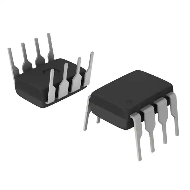
8 NC
C 1
A 2
K2
K1
7 NC
C 3
6 C
A 4
5 A
i179026_2
V
D E
Couples AC and DC signals
0.01 % servo linearity
Wide bandwidth, > 200 kHz
High gain stability, ± 0.005 %/°C typically
Low input-output capacitance
Low power consumption, < 15 mW
Isolation rated voltage 4420 VRMS
Internal insulation distance, > 0.4 mm
Material categorization: for definitions of compliance
please see www.vishay.com/doc?99912
APPLICATIONS
•
•
•
•
•
DESCRIPTION
The IL300 linear optocoupler consists of an AlGaAs IRLED
irradiating an isolated feedback and an output PIN
photodiode in a bifurcated arrangement. The feedback
photodiode captures a percentage of the LEDs flux and
generates a control signal (IP1) that can be used to servo the
LED drive current. This technique compensates for the
LED’s non-linear, time, and temperature characteristics.
The output PIN photodiode produces an output signal (IP2)
that is linearly related to the servo optical flux created by the
LED.
The time and temperature stability of the input-output
coupler gain (K3) is insured by using matched PIN
photodiodes that accurately track the output flux of the LED.
Power supply feedback voltage / current
Medical sensor isolation
Audio signal interfacing
Isolated process control transducers
Digital telephone isolation
AGENCY APPROVALS
•
•
•
•
•
•
UL
cUL
DIN EN 60747-5-5 (VDE 0884-5) available with option 1
BSI
FIMKO
CQC
ORDERING INFORMATION
I
L
3
0
0
-
D
PART NUMBER
E
F
G
-
X
K3 BIN
0
#
#
PACKAGE OPTION
DIP-8
Option 6
7.62 mm
10.16 mm
T
TAPE
AND
REEL
Option 7
> 0.1 mm
> 0.7 mm
AGENCY
CERTIFIED /
PACKAGE
UL, cUL,
BSI, FIMKO
K3 BIN
0.557 to 1.618
0.765 to 1.181
0.851 to 1.181
0.765 to 0.955
0.851 to 1.061
IL300
IL300-DEFG
-
-
IL300-EF
IL300-X006
IL300-DEFG-X006
-
-
IL300-EF-X006
DIP-8
DIP-8, 400 mil,
option 6
Option 9
SMD-8, option 7
IL300-X007T(1) IL300-DEFG-X007T(1)
SMD-8, option 9
IL300-X009T(1) IL300-DEFG-X009T(1)
VDE, UL,
BSI, FIMKO
0.557 to 1.618
DIP-8
DIP-8, 400 mil,
option 6
0.945 to 1.181 0.851 to 0.955 0.945 to 1.061
-
IL300-E
IL300-FG-X006 IL300-E-X006
IL300-F
IL300-F-X006
IL300-EFG-X007
IL300-DE-X007T IL300-EF-X007T(1) IL300-FG-X007T
-
-
IL300-EF-X009T(1)
0.765 to 1.181
0.851 to 1.181
0.765 to 0.955
0.851 to 1.061
IL300-X001
IL300-DEFG-X001
-
-
IL300-EF-X001
-
IL300-E-X001
IL300-F-X001
IL300-X016
IL300-DEFG-X016 IL300-EFG-X016
-
IL300-EF-X016
-
-
IL300-F-X016
-
IL300-E-X007T IL300-F-X007T(1)
-
IL300-F-X009T(1)
0.945 to 1.181 0.851 to 0.955 0.945 to 1.061
SMD-8, option 7 IL300-X017 IL300-DEFG-X017T(1)
-
-
IL300-EF-X017T(1)
-
IL300-E-X017T IL300-F-X017T(1)
SMD-8, option 9
-
-
-
-
IL300-E-X009T IL300-F-X019T(1)
-
-
Note
(1) Also available in tubes, do not put “T” on the end
Rev. 2.0, 05-Mar-18
Document Number: 83622
1
For technical questions, contact: optocoupleranswers@vishay.com
THIS DOCUMENT IS SUBJECT TO CHANGE WITHOUT NOTICE. THE PRODUCTS DESCRIBED HEREIN AND THIS DOCUMENT
ARE SUBJECT TO SPECIFIC DISCLAIMERS, SET FORTH AT www.vishay.com/doc?91000
�IL300
www.vishay.com
Vishay Semiconductors
ABSOLUTE MAXIMUM RATINGS (Tamb = 25 °C, unless otherwise specified)
PARAMETER
TEST CONDITION
SYMBOL
VALUE
UNIT
INPUT
Power dissipation
Pdiss
Derate linearly from 25 °C
160
mW
2.13
mW/°C
Forward current
IF
60
mA
Surge current (pulse width < 10 μs)
IPK
250
mA
Reverse voltage
VR
5
V
Thermal resistance
Rth
470
K/W
Tj
100
°C
Junction temperature
OUTPUT
Power dissipation
Pdiss
Derate linearly from 25 °C
50
mW
0.65
mW/°C
Reverse voltage
VR
50
V
Thermal resistance
Rth
1500
K/W
Tj
100
°C
Ptot
210
mW
2.8
mW/°C
Junction temperature
COUPLER
Total package dissipation at 25 °C
Derate linearly from 25 °C
Storage temperature
Tstg
-55 to +150
°C
Operating temperature
Tamb
-55 to +100
°C
Note
• Stresses in excess of the absolute maximum ratings can cause permanent damage to the device. Functional operation of the device is not
implied at these or any other conditions in excess of those given in the operational sections of this document. Exposure to absolute
maximum ratings for extended periods of the time can adversely affect reliability
ELECTRICAL CHARACTERISTICS (Tamb = 25 °C, unless otherwise specified)
PARAMETER
TEST CONDITION
SYMBOL
MIN.
TYP.
MAX.
UNIT
INPUT (LED EMITTER)
IF = 10 mA
Forward voltage
VF temperature coefficient
Reverse current
Junction capacitance
Dynamic resistance
VF
-
1.25
1.50
V
ΔVF/Δ°C
-
-2.2
-
mV/°C
VR = 5 V
IR
-
1
-
μA
VF = 0 V, f = 1 MHz
Cj
-
15
-
pF
IF = 10 mA
ΔVF/ΔIF
-
6
-
Ω
Vdet = -15 V, IF = 0 A
ID
-
1
25
nA
IF = 10 mA
VD
-
500
-
mV
μA
OUTPUT
Dark current
Open circuit voltage
Short circuit current
Junction capacitance
Noise equivalent power
IF = 10 mA
ISC
-
120
-
VF = 0 V, f = 1 MHz
Cj
-
12
-
pF
Vdet = 15 V
NEP
-
4 x 10-14
-
W/√Hz
-
1
-
pF
K1
0.006
0.012
0.017
COUPLER
Input-output capacitance
K1, servo gain (IP1/IF)
VF = 0 V, f = 1 MHz
IF = 10 mA, Vdet = -15 V
Servo photocurrent (1)(2)
IF = 10 mA, Vdet = -15 V
IP1
-
120
-
K2, forward gain (IP2/IF)
IF = 10 mA, Vdet = -15 V
K2
0.006
0.012
0.017
Forward current
IF = 10 mA, Vdet = -15 V
IP2
-
120
-
μA
K3, transfer gain
(K2/K1) (1)(2)
Transfer gain stability
Transfer gain linearity
Rev. 2.0, 05-Mar-18
μA
IF = 10 mA, Vdet = -15 V
K3
0.56
1
1.65
K2/K1
IF = 10 mA, Vdet = -15 V
ΔK3/ΔTA
-
± 0.005
± 0.15
%/°C
IF = 1 mA to 10 mA
ΔK3
-
± 0.25
-
%
-
± 0.5
-
%
IF = 1 mA to 10 mA, Tamb = 0 °C to 75 °C
Document Number: 83622
2
For technical questions, contact: optocoupleranswers@vishay.com
THIS DOCUMENT IS SUBJECT TO CHANGE WITHOUT NOTICE. THE PRODUCTS DESCRIBED HEREIN AND THIS DOCUMENT
ARE SUBJECT TO SPECIFIC DISCLAIMERS, SET FORTH AT www.vishay.com/doc?91000
�IL300
www.vishay.com
Vishay Semiconductors
ELECTRICAL CHARACTERISTICS (Tamb = 25 °C, unless otherwise specified)
PARAMETER
TEST CONDITION
SYMBOL
MIN.
TYP.
MAX.
UNIT
IFq = 10 mA, MOD = ± 4 mA, RL = 50 Ω
BW (-3 db)
-
200
-
kHz
-
-45
-
Deg.
PHOTOCONDUCTIVE OPERATION
Frequency response
Phase response at 200 kHz
Vdet = -15 V
Notes
• Minimum and maximum values were tested requirements. Typical values are characteristics of the device and are the result of engineering
evaluation. Typical values are for information only and are not part of the testing requirements
(1) Bin sorting: K3 (transfer gain) is sorted into bins that are ± 6 %, as follows:
Bin A = 0.557 to 0.626
Bin B = 0.620 to 0.696
Bin C = 0.690 to 0.773
Bin D = 0.765 to 0.859
Bin E = 0.851 to 0.955
Bin F = 0.945 to 1.061
Bin G = 1.051 to 1.181
Bin H = 1.169 to 1.311
Bin I = 1.297 to 1.456
Bin J = 1.442 to 1.618
K3 = K2/K1. K3 is tested at IF = 10 mA, Vdet = -15 V
(2) Bin categories: All IL300s are sorted into a K3 bin, indicated by an alpha character that is marked on the part. The bins range from “A”
through “J”.
The IL300 is shipped in tubes of 50 each. Each tube contains only one category of K3. The category of the parts in the tube is marked on
the tube label as well as on each individual part
(3) Category options: standard IL300 orders will be shipped from the categories that are available at the time of the order. Any of the ten
categories may be shipped. For customers requiring a narrower selection of bins, the bins can be grouped together as follows:
IL300-DEFG: order this part number to receive categories D, E, F, G only
IL300-EF: order this part number to receive categories E, F only
IL300-E: order this part number to receive category E only
SWITCHING CHARACTERISTICS
PARAMETER
TEST CONDITION
SYMBOL
MIN.
TYP.
MAX.
UNIT
tr
-
1
-
μs
tf
-
1
-
μs
Rise time
tr
-
1.75
-
μs
Fall time
tf
-
1.75
-
μs
UNIT
ΔIF = 2 mA, IFq = 10 mA
Switching time
COMMON MODE TRANSIENT IMMUNITY
PARAMETER
TEST CONDITION
SYMBOL
MIN.
TYP.
MAX.
Common mode capacitance
VF = 0 V, f = 1 MHz
CCM
-
0.5
-
pF
f = 60 Hz, RL = 2.2 kΩ
CMRR
-
130
-
dB
TEST CONDITION
SYMBOL
Common mode rejection ratio
SAFETY AND INSULATION RATINGS
PARAMETER
Climatic classification
According to IEC 68 part 1
Comparative tracking index
VALUE
UNIT
55 / 100 / 21
CTI
175
VISO
4420
VRMS
Maximum transient isolation voltage
VIOTM
10 000
Vpeak
Maximum repetitive peak isolation voltage
VIORM
890
Vpeak
VIO = 500 V, Tamb = 25 °C
RIO
≥ 1012
Ω
VIO = 500 V, Tamb = 100 °C
RIO
≥ 1011
Ω
Output safety power
PSO
400
mW
Input safety current
ISI
275
mA
Safety temperature
TS
175
°C
≥7
mm
≥7
mm
≥ 0.4
mm
Maximum rated withstanding isolation voltage
Isolation resistance
t = 1 min
Creepage distance
Clearance distance
Insulation thickness
DTI
Note
• As per IEC 60747-5-5, § 7.4.3.8.2, this optocoupler is suitable for “safe electrical insulation” only within the safety ratings. Compliance with
the safety ratings shall be ensured by means of protective circuits
Rev. 2.0, 05-Mar-18
Document Number: 83622
3
For technical questions, contact: optocoupleranswers@vishay.com
THIS DOCUMENT IS SUBJECT TO CHANGE WITHOUT NOTICE. THE PRODUCTS DESCRIBED HEREIN AND THIS DOCUMENT
ARE SUBJECT TO SPECIFIC DISCLAIMERS, SET FORTH AT www.vishay.com/doc?91000
�IL300
www.vishay.com
Vishay Semiconductors
TYPICAL CHARACTERISTICS (Tamb = 25 °C, unless otherwise specified)
Axis Title
Axis Title
10000
100
10000
0.025
100
1
1000
0.015
Tamb = 25 °C
0.010
1.4
10
0
10
1.2
0
1.6
10
20
30
40
50
VF - Forward Voltage (V)
IF - Forward Current (mA)
Fig. 1 - Forward Current vs. Forward Voltage
Fig. 4 - Servo Gain vs. Forward Current
Axis Title
Axis Title
10000
Tamb = -55 °C
1000
1st line
2nd line
Tamb = 0 °C
300
Tamb = 25 °C
200
100
Tamb = 85 °C
100
Tamb = 100 °C
10
0
0
5
10
15
20
Normalized to:
IF = 10 mA, Tamb = 25 °C
1.03
1.02
Tamb = 85 °C
Tamb = 100 °C
1000
1.01
1st line
2nd line
400
10000
1.04
2nd line
NK3 - Normalized Transfer Gain (K1/K2)
500
1.00
0.99
Tamb = -55 °C
Tamb = 25 °C
100
Tamb = 0 °C
0.98
0.97
10
0.96
25
0
10
20
30
40
50
IF - Forward Current (mA)
IF - Forward Current (mA)
Fig. 2 - Servo Photocurrent vs. Forward Current
Fig. 5 - Normalized Transfer Gain vs. Forward Current
Axis Title
Axis Title
10000
8
Normalized to:
IF = 10 mA,
VD = -15 V,
Tamb = 25 °C
6
1000
4
1st line
2nd line
Tamb = 25 °C
5
Tamb = 0 °C
3
RL = 1 kΩ
1
Tamb = -55 °C
100
2
2nd line
Voltage Gain (dB)
7
10000
2
1000
0
-1
1st line
2nd line
2nd line
IP1 - Servo Photocurrent (μA)
100
Tamb = 85 °C
Tamb = 100 °C
0.005
1.0
1st line
2nd line
1000
2nd line
K1 - Servo Gain (IP1/IF)
Tamb = 25 °C
10
0.1
2nd line
NIP1 - Normalized Photodiode Current
Tamb = 0 °C
0.020
1st line
2nd line
2nd line
IF - Forward Current (mA)
Tamb = -55 °C
RL = 10 kΩ
100
-2
Tamb = 85 °C
-3
1
Tamb = 100 °C
10
0
0
10
20
30
40
50
-4
0.01
IF = 10 mA,
IF(MOD) = ± 2 mA
0.1
1
10
100
IF - Forward Current (mA)
f - Frequency (kHz)
Fig. 3 - Normalized Photodiode Current vs. Forward Current
Fig. 6 - Voltage Gain vs. Frequency
(2 mA)
Rev. 2.0, 05-Mar-18
10
1000
Document Number: 83622
4
For technical questions, contact: optocoupleranswers@vishay.com
THIS DOCUMENT IS SUBJECT TO CHANGE WITHOUT NOTICE. THE PRODUCTS DESCRIBED HEREIN AND THIS DOCUMENT
ARE SUBJECT TO SPECIFIC DISCLAIMERS, SET FORTH AT www.vishay.com/doc?91000
�IL300
www.vishay.com
Vishay Semiconductors
Axis Title
Axis Title
10000
-1
100
-2
-3
IF = 10 mA
IFmod = ± 4 mA
RL = 50 Ω
-4
0.01
0.1
1
10
100
10
1000
-20
1000
-40
1st line
2nd line
1000
1st line
2nd line
2nd line
Voltage Gain (dB)
1
0
10000
0
2nd line
Common Mode Rejection Ratio (dB)
2
-60
100
-80
-100
-120
0.1
1
Fig. 7 - Voltage Gain vs. Frequency
Fig. 9 - Common-Mode Rejection Ratio vs. Frequency
Axis Title
1st line
2nd line
-4
100
-6
IF = 10 mA
IFmod = ± 4 mA
RL = 50 Ω
0.1
1
10
100
10
1000
10000
14
f = 1 MHz
12
10
1000
1st line
2nd line
1000
-2
2nd line
Cj - Photodiode Junction Capacitance (pF)
10000
0
2nd line
Phase Angle (°)
10
1000
f - Frequency (kHz)
Axis Title
-10
0.01
100
f - Frequency (kHz)
2
-8
10
8
6
100
4
2
10
0
0
2
4
6
8
10
f - Frequency (kHz)
VR - Reverse Voltage (V)
Fig. 8 - Phase Angle vs. Frequency
Fig. 10 - Photodiode Junction Capacitance vs. Reverse Voltage
Rev. 2.0, 05-Mar-18
Document Number: 83622
5
For technical questions, contact: optocoupleranswers@vishay.com
THIS DOCUMENT IS SUBJECT TO CHANGE WITHOUT NOTICE. THE PRODUCTS DESCRIBED HEREIN AND THIS DOCUMENT
ARE SUBJECT TO SPECIFIC DISCLAIMERS, SET FORTH AT www.vishay.com/doc?91000
�IL300
www.vishay.com
Vishay Semiconductors
PACKAGE DIMENSIONS (in millimeters)
Pin one ID
0.527
0.889
3.302
3.810
6.096
6.604
2.540
0.46
0.58
1.016
1.270
1
8
2
7
3
6
4
5
4°
1.270
9.652
10.16
7.112
8.382
0.254 ref.
7.62 typ.
0.254 ref.
0.508 ref.
3°
9
ISO method A
10°
0.203
0.305
i178010
2.794
3.302
Option 6
Option 7
Option 9
10.36
9.96
7.62 typ.
9.53
10.03
7.8
7.4
7.62 ref.
0.7
4.6
4.1
0.102
0.249
8 min.
0.35
0.25
0.25 typ.
0.51
1.02
8.4 min.
15° max.
8 min.
10.16
10.92
10.3 max.
18450
PACKAGE MARKING (example of IL300-E-X001)
IL300-E
V YWW 68
Rev. 2.0, 05-Mar-18
Document Number: 83622
6
For technical questions, contact: optocoupleranswers@vishay.com
THIS DOCUMENT IS SUBJECT TO CHANGE WITHOUT NOTICE. THE PRODUCTS DESCRIBED HEREIN AND THIS DOCUMENT
ARE SUBJECT TO SPECIFIC DISCLAIMERS, SET FORTH AT www.vishay.com/doc?91000
�Legal Disclaimer Notice
www.vishay.com
Vishay
Disclaimer
ALL PRODUCT, PRODUCT SPECIFICATIONS AND DATA ARE SUBJECT TO CHANGE WITHOUT NOTICE TO IMPROVE
RELIABILITY, FUNCTION OR DESIGN OR OTHERWISE.
Vishay Intertechnology, Inc., its affiliates, agents, and employees, and all persons acting on its or their behalf (collectively,
“Vishay”), disclaim any and all liability for any errors, inaccuracies or incompleteness contained in any datasheet or in any other
disclosure relating to any product.
Vishay makes no warranty, representation or guarantee regarding the suitability of the products for any particular purpose or
the continuing production of any product. To the maximum extent permitted by applicable law, Vishay disclaims (i) any and all
liability arising out of the application or use of any product, (ii) any and all liability, including without limitation special,
consequential or incidental damages, and (iii) any and all implied warranties, including warranties of fitness for particular
purpose, non-infringement and merchantability.
Statements regarding the suitability of products for certain types of applications are based on Vishay’s knowledge of
typical requirements that are often placed on Vishay products in generic applications. Such statements are not binding
statements about the suitability of products for a particular application. It is the customer’s responsibility to validate that a
particular product with the properties described in the product specification is suitable for use in a particular application.
Parameters provided in datasheets and / or specifications may vary in different applications and performance may vary over
time. All operating parameters, including typical parameters, must be validated for each customer application by the customer’s
technical experts. Product specifications do not expand or otherwise modify Vishay’s terms and conditions of purchase,
including but not limited to the warranty expressed therein.
Except as expressly indicated in writing, Vishay products are not designed for use in medical, life-saving, or life-sustaining
applications or for any other application in which the failure of the Vishay product could result in personal injury or death.
Customers using or selling Vishay products not expressly indicated for use in such applications do so at their own risk.
Please contact authorized Vishay personnel to obtain written terms and conditions regarding products designed for
such applications.
No license, express or implied, by estoppel or otherwise, to any intellectual property rights is granted by this document
or by any conduct of Vishay. Product names and markings noted herein may be trademarks of their respective owners.
© 2019 VISHAY INTERTECHNOLOGY, INC. ALL RIGHTS RESERVED
Revision: 01-Jan-2019
1
Document Number: 91000
�