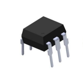
IL4116, IL4117, IL4118
www.vishay.com
Vishay Semiconductors
Optocoupler, Phototriac Output, Zero Crossing,
Very Low Input Current
FEATURES
A 1
6 MT2
C 2
5 NC
NC 3
ZCC*
•
•
•
•
•
•
4 MT1
*Zero crossing circuit
Low trigger current IFT = 0.7 mA (typ.)
ITRMS = 300 mA
High static dV/dt ≥ 10 000 V/μs
Load voltage up to 800 V
Zero voltage crossing detector
Material categorization:
for definitions of compliance please see
www.vishay.com/doc?99912
APPLICATIONS
•
•
•
•
•
23128
LINKS TO ADDITIONAL RESOURCES
3D 3D
3D Models
Design Tools
Related
Documents
Models
Footprints
Solid-state relay
Lighting controls
Temperature controls
Solenoid / valve controls
AC motor drives / starters
AGENCY APPROVALS
•
•
•
•
•
Schematics
DESCRIPTION
The IL4116, IL4117, and IL4118 product family consists of
an optically coupled GaAs IRLED to a photosensitive
thyristor system with integrated noise suppression and zero
crossing circuit.
The thyristor system enables low trigger currents of 0.7 mA
and features a dV/dt ratio of greater than 10 kV/μs and load
voltages up to 800 V.
The IL4116, IL4117, and IL4118 product family is a perfect
microcontroller friendly solution to isolate low voltage logic
from high voltage 120 VAC, 240 VAC, and 380 VAC lines and
to control resistive, inductive, or capacitive AC loads like
motors, solenoids, high power thyristors or TRIACs, and
solid-state relays.
UL
cUL
DIN EN 60747-5-5 (VDE 0884-5) available with option 1
CSA
FIMKO
ORDERING INFORMATION
I
L
4
1
1
#
-
X
PART NUMBER
0
#
#
PACKAGE OPTION
DIP
Option 6
7.62 mm
10.16 mm
Option 7
Option 9
T
TAPE
AND
REEL
> 0.7 mm
AGENCY CERTIFIED / PACKAGE
UL, cUL, FIMKO
DIP-6
DIP-6, 400 mil, option 6
> 0.1 mm
PEAK OFF-STATE VOLTAGE VDRM (V)
600
700
800
IL4116
IL4117
IL4118
-
-
IL4118-X006
SMD-6, option 7
IL4116-X007T (1)
IL4117-X007
IL4118-X007T (1)
SMD-6, option 9
IL4116-X009T
-
IL4118-X009T
600
700
800
-
-
IL4118-X017
VDE, UL, cUL, FIMKO
SMD-6, option 7
Notes
• Additional options may be possible, please contact sales office
(1) Also available in tubes, do not put T on the end
Rev. 2.0, 11-Nov-2021
Document Number: 83628
1
For technical questions, contact: optocoupleranswers@vishay.com
THIS DOCUMENT IS SUBJECT TO CHANGE WITHOUT NOTICE. THE PRODUCTS DESCRIBED HEREIN AND THIS DOCUMENT
ARE SUBJECT TO SPECIFIC DISCLAIMERS, SET FORTH AT www.vishay.com/doc?91000
�IL4116, IL4117, IL4118
www.vishay.com
Vishay Semiconductors
ABSOLUTE MAXIMUM RATINGS (Tamb = 25 °C, unless otherwise specified)
PARAMETER
TEST CONDITION
PART
SYMBOL
VALUE
UNIT
INPUT
Reverse voltage
VR
6
V
Forward current
IF
60
mA
Surge current
IFSM
2.5
A
Power dissipation
Pdiss
100
mW
Derate linearly from 25 °C
1.33
mW/°C
Rth
750
°C/W
IL4116
VDRM
600
V
IL4117
VDRM
700
V
IL4118
VDRM
800
V
IDRM
300
mA
3
A
Pdiss
500
mW
6.6
mW/°C
Rth
150
°C/W
Storage temperature
Tstg
-55 to +150
°C
Operating temperature
Tamb
-55 to +100
°C
Tsld
260
°C
Thermal resistance
OUTPUT
Peak off-state voltage
RMS on-state current
Single cycle surge
Power dissipation
Derate linearly from 25 °C
Thermal resistance
COUPLER
Lead soldering temperature
5s
Note
• Stresses in excess of the absolute maximum ratings can cause permanent damage to the device. Functional operation of the device is not
implied at these or any other conditions in excess of those given in the operational sections of this document. Exposure to absolute
maximum ratings for extended periods of the time can adversely affect reliability
Rev. 2.0, 11-Nov-2021
Document Number: 83628
2
For technical questions, contact: optocoupleranswers@vishay.com
THIS DOCUMENT IS SUBJECT TO CHANGE WITHOUT NOTICE. THE PRODUCTS DESCRIBED HEREIN AND THIS DOCUMENT
ARE SUBJECT TO SPECIFIC DISCLAIMERS, SET FORTH AT www.vishay.com/doc?91000
�IL4116, IL4117, IL4118
www.vishay.com
Vishay Semiconductors
ELECTRICAL CHARACTERISTICS (Tamb = 25 °C, unless otherwise specified)
PARAMETER
TEST CONDITION
PART
SYMBOL
MIN.
TYP.
MAX.
UNIT
INPUT
Forward voltage
IF = 20 mA
VF
-
1.3
1.5
V
Breakdown voltage
IR = 10 μA
VBR
6
30
-
V
VR = 6 V
IR
-
0.1
10
μA
VF = 0 V, f = 1 MHz
CO
-
40
-
pF
RthjI
-
750
-
°C/W
IL4116
VDRM
600
650
-
V
IL4117
VDRM
700
750
-
V
Reverse current
Capacitance
Thermal resistance, junction to lead
OUTPUT
Repetitive peak off-state voltage
IDRM = 100 μA
IL4118
VDRM
800
850
-
V
IL4116
VD(RMS)
424
460
-
V
IL4117
VD(RMS)
494
536
-
V
IL4118
VD(RMS)
565
613
-
V
VD = 600, Tamb = 100 °C
ID(RMS)
-
10
100
μA
On-state voltage
IT = 300 mA
VTM
-
1.7
3
V
On-state current
PF = 1, VT(RMS) = 1.7 V
ITM
-
-
300
mA
f = 50 Hz
ITSM
-
-
3
A
Holding current
VT = 3 V
IH
-
65
200
μA
Latching current
VT = 2.2 V
IL
-
-
500
μA
LED trigger current
VAK = 5 V
IFT
-
0.7
1.3
mA
Off-state voltage
ID(RMS) = 70 μA
Off-state current
Surge (non-repetitive, on-state current)
Zero cross inhibit voltage
IF = rated IFT
VIH
-
15
25
V
VRM, VDM = 400 VAC
dV/dtcr
10 000
-
-
V/μs
VRM, VDM = 400 VAC,
Tamb = 80 °C
dV/dtcr
-
2000
-
V/μs
VD = 230 VRMS,
ID = 300 mARMS, TJ = 25 °C
dV/dtcrq
-
8
-
V/μs
VD = 230 VRMS,
ID = 300 mARMS, TJ = 85 °C
dV/dtcrq
-
7
-
V/μs
VD = 230 VRMS,
ID = 300 mARMS, TJ = 25 °C
dV/dtcrq
-
12
-
A/ms
RthjI
-
150
-
°C/W
dV(IO)/dt
10 000
-
-
V/μs
CIO
-
0.8
-
pF
CCM
-
0.01
-
pF
Critical rate of rise off-state voltage
Critical rate of rise of voltage at current
commutation
Critical rate of rise of on-state current
commutation
Thermal resistance, junction to lead
COUPLER
Critical state of rise of coupler
input-output voltage
IT = 0 A, VRM = VDM = 424 VAC
Capacitance (input to output)
f = 1 MHz, VIO = 0 V
Common mode coupling capacitance
Note
• Minimum and maximum values are testing requirements. Typical values are characteristics of the device and are the result of engineering
evaluation. Typical values are for information only and are not part of the testing requirements
SWITCHING CHARACTERISTICS
PARAMETER
TEST CONDITION
SYMBOL
MIN.
TYP.
MAX.
UNIT
Turn-on time
VRM = VDM = 424 VAC
ton
-
35
-
μs
Turn-off time
PF = 1, IT = 300 mA
toff
-
50
-
μs
Rev. 2.0, 11-Nov-2021
Document Number: 83628
3
For technical questions, contact: optocoupleranswers@vishay.com
THIS DOCUMENT IS SUBJECT TO CHANGE WITHOUT NOTICE. THE PRODUCTS DESCRIBED HEREIN AND THIS DOCUMENT
ARE SUBJECT TO SPECIFIC DISCLAIMERS, SET FORTH AT www.vishay.com/doc?91000
�IL4116, IL4117, IL4118
www.vishay.com
Vishay Semiconductors
SAFETY AND INSULATION RATINGS
PARAMETER
TEST CONDITION
Climatic classification
SYMBOL
VALUE
According to IEC 68 part 1
UNIT
55 / 100 / 21
Comparative tracking index
CTI
175
VISO
4420
Maximum transient isolation voltage
VIOTM
8000
Vpeak
Maximum repetitive peak isolation voltage
VIORM
890
Vpeak
VIO = 500 V, Tamb = 25 °C
RIO
≥ 1012
Ω
VIO = 500 V, Tamb = 100 °C
RIO
≥ 1011
Ω
Output safety power
PSO
500
mW
Input safety current
ISI
250
mA
TS
Maximum rated withstanding isolation voltage
t = 1 min
Isolation resistance
Safety temperature
Creepage distance
Clearance distance
VRMS
175
°C
DIP-6; SMD-6, option 7; SMD-6, option 9
≥7
mm
DIP-6, 400 mil, option 6
≥8
mm
DIP-6; SMD-6, option 7; SMD-6, option 9
≥7
mm
DIP-6, 400 mil, option 6
≥8
mm
≥ 0.4
mm
Insulation thickness
DTI
Note
• As per IEC 60747-5-5, § 7.4.3.8.2, this optocoupler is suitable for “safe electrical insulation” only within the safety ratings. Compliance with
the safety ratings shall be ensured by means of protective circuits
TYPICAL CHARACTERISTICS (Tamb = 25 °C, unless otherwise specified)
10 000
If(pk) - Peak LED Current (mA)
35
IF - LED Current (mA)
30
25
20
15
10
5
0
1.0
iil4116_01
1.1
1.2
1.3
1000
100
DF = τ/t
101
Fig. 3 - Peak LED Current vs. Duty Factor, τ
150
1.3
PLED - LED Power (mW)
1.4
VF - Forward Voltage (V)
t
t - LED Pulse Duration (s)
iil4116_03
Fig. 1 - LED Forward Current vs. Forward Voltage
0.005
0.01
0.02
0.05
0.1
0.2
0.5
10
10-6 10-5 10-4 10-3 10-2 10-1 100
1.4
VF - LED Forward Voltage (V)
τ
Duty Factor
TA = - 55 °C
1.2
TA = 25 °C
1.1
1.0
0.9
TA = 100 °C
100
50
0.8
0.7
0.1
iil4116_02
1
10
100
IF - Forward Current (mA)
Fig. 2 - Forward Voltage vs. Forward Current
Rev. 2.0, 11-Nov-2021
0
-60
-40
-20
0
20
40
60
80
100
TA - Ambient Temperature (°C)
iil4116_04
Fig. 4 - Maximum LED Power Dissipation
Document Number: 83628
4
For technical questions, contact: optocoupleranswers@vishay.com
THIS DOCUMENT IS SUBJECT TO CHANGE WITHOUT NOTICE. THE PRODUCTS DESCRIBED HEREIN AND THIS DOCUMENT
ARE SUBJECT TO SPECIFIC DISCLAIMERS, SET FORTH AT www.vishay.com/doc?91000
�IL4116, IL4117, IL4118
www.vishay.com
Vishay Semiconductors
300
400
PLED - LED Power (mW)
IT - On-Site Current - mARMS
500
300
200
100
0
-100
-200
-300
250
200
150
100
50
-400
-500
-3
-2
-1
0
1
2
3
0
-60 -40 -20
VT - On-State Voltage - VRMS
iil4116_05
iil4116_06
Fig. 5 - On-State Terminal Voltage vs. Terminal Current
0
20
40
60
80 100
TA - Ambient Temperature (°C)
Fig. 6 - Maximum Output Power Dissipation
TRIGGER CURRENT VS. TEMPERATURE AND VOLTAGE
The trigger current of the IL4116, IL4117, IL4118 has a
positive temperature gradient and also is dependent on the
terminal voltage as shown as the fig. 7.
2.5
100 °C
IFT (mA)
2.0
85 °C
1.5
25 °C
1.0
50 °C
0.5
0.0
0
50
21611
100
150 200
250
300
350
VRMS (V)
Fig. 7 - Trigger Current vs.
Temperature and Operating Voltage (50 Hz)
For the operating voltage 250 VRMS over the temperature
range -40 °C to +85 °C, the IF should be at least 2.3 x of the
IFT1 (1.3 mA, max.).
Considering -30 % degradation over time, the trigger
current minimum is IF = 1.3 x 2.3 x 130 % = 4 mA
Rev. 2.0, 11-Nov-2021
Document Number: 83628
5
For technical questions, contact: optocoupleranswers@vishay.com
THIS DOCUMENT IS SUBJECT TO CHANGE WITHOUT NOTICE. THE PRODUCTS DESCRIBED HEREIN AND THIS DOCUMENT
ARE SUBJECT TO SPECIFIC DISCLAIMERS, SET FORTH AT www.vishay.com/doc?91000
�IL4116, IL4117, IL4118
www.vishay.com
Vishay Semiconductors
INDUCTIVE AND RESISTIVE LOADS
For inductive loads, there is phase shift between voltage and current, shown in the Fig. 8.
IF(on)
IF(on)
IF(off)
IF(off)
AC line
voltage
AC line
voltage
AC current
through
triac
AC current
through
triac
Commutating dV/dt
Commutating dV/dt
Voltage
across triac
21607
Voltage
across triac
Resistive load
Inductive load
Fig. 8 - Waveforms of Resistive and Inductive Loads
Lost Control to Turn Off
If the commutating dV/dt is too high, more than its critical
rate (dV/dtcrq), the triac may resume conduction even if the
LED drive current IF is off and control is lost.
In order to achieve control with certain inductive loads of
power factors is less than 0.8, the rate of rise in voltage
(dV/dt) must be limited by a series RC network placed in
parallel with the power handling triac. The RC network is
called snubber circuit. Note that the value of the capacitor
increases as a function of the load current as shown in fig. 9.
1
CS - Shunt Capacitance (µF)
The voltage across the triac will rise rapidly at the time the
current through the power handling triac falls below the
holding current and the triac ceases to conduct. The rise
rate of voltage at the current commutation is called
commutating dV/dt. There would be two potential problems
for ZC phototriac control if the commutating dV/dt is too
high. One is lost control to turn off, another is failed to keep
the triac on.
C S (µF) = 0.0032 (µF) x 10 ^ (0.0066 IL (mA))
0.1
0.01
PF = 0.3
IF = 2.0 mA
0.001
0
Fig. 9 - Shunt Capacitance vs. Load Current vs. Power Factor
Failed to Keep On
This hold-off condition can be eliminated by using a snubber
and also by providing a higher level of LED drive current. The
higher LED drive provides a larger photocurrent which
causes the triac to turn-on before the commutating spike
has activated the zero cross detection circuit. Fig. 10 shows
the relationship of the LED current for power factors of less
than 1.0. The curve shows that if a device requires 1.5 mA
for a resistive load, then 1.8 times (2.7 mA) that amount
would be required to control an inductive load whose power
factor is less than 0.3 without the snubber to dump the
spike.
Rev. 2.0, 11-Nov-2021
2.0
NIFth - Normalized LED
Trigger Current
As a zero-crossing phototriac, the commutating dV/dt
spikes can inhibit one half of the TRIAC from keeping on If
the spike potential exceeds the inhibit voltage of the zero
cross detection circuit, even if the LED drive current IF is on.
50 100 150 200 250 300 350 400
I L - Load Current (mA)
iil4116_07
1.8
1.6
1.4
1.2
1.0
IFth normalized to IFth at PF = 1.0
0.8
0
0.2
0.4
0.6
0.8
1.0
1.2
PF - Power Factor
iil4116_08-1
Fig. 10 - Normalized LED Trigger Current
Document Number: 83628
6
For technical questions, contact: optocoupleranswers@vishay.com
THIS DOCUMENT IS SUBJECT TO CHANGE WITHOUT NOTICE. THE PRODUCTS DESCRIBED HEREIN AND THIS DOCUMENT
ARE SUBJECT TO SPECIFIC DISCLAIMERS, SET FORTH AT www.vishay.com/doc?91000
�IL4116, IL4117, IL4118
www.vishay.com
Vishay Semiconductors
APPLICATIONS
Indirect switching operation:
Direct switching operation:
The IL4116, IL4117, IL4118 switch acts here as an isolated
driver and thus enables the driving of power thyristors and
power triacs by microprocessors. Fig. 12 shows a basic
driving circuit of inductive load. The resister R1 limits the
driving current pulse which should not exceed the maximum
permissible surge current of the IL4116, IL4117, IL4118.
The resister RG is needed only for very sensitive thyristors or
triacs from being triggered by noise or the inhibit current.
The IL4116, IL4117, IL4118 isolated switch is mainly suited
to control synchronous motors, valves, relays and
solenoids. Fig. 11 shows a basic driving circuit. For resistive
load the snubber circuit RS CS can be omitted due to the
high static dV/dt characteristic.
1
Hot
6
Control
RS
2
CS
ZC
3
R1
360
220/240
VAC
5
1
Hot
6
Control
4
2
U1
5
Nutral
21608-1
3
4
CS
RG
330
U1
Fig. 11 - Basic Direct Load Driving Circuit
220/240
VAC
RS
ZC
Inductive load
Inductive load
Nutral
21609-1
Fig. 12 - Basic Power Triac Driver Circuit
PACKAGE DIMENSIONS (in millimeters)
3
2
1
4
5
6
Pin one ID
6.4 ± 0.1
ISO method A
8.6 ± 0.1
7.62 typ.
1.2 ± 0.1
1 min.
3.555 ± 0.255
18°
4° typ.
2.95 ± 0.5
0.8 min.
0.85 ± 0.05
0.5 ± 0.05
0.25 typ.
3° to 9°
7.62 to 8.81
i178004
2.54 typ.
Option 6
Option 7
Option 9
10.36
9.96
7.62 typ.
9.53
10.03
7.8
7.4
7.62 ref.
0.7
4.6
4.1
0.102
0.249
8 min.
0.35
0.25
0.25 typ.
0.51
1.02
8.4 min.
15° max.
8 min.
10.16
10.92
Rev. 2.0, 11-Nov-2021
10.3 max.
18450
Document Number: 83628
7
For technical questions, contact: optocoupleranswers@vishay.com
THIS DOCUMENT IS SUBJECT TO CHANGE WITHOUT NOTICE. THE PRODUCTS DESCRIBED HEREIN AND THIS DOCUMENT
ARE SUBJECT TO SPECIFIC DISCLAIMERS, SET FORTH AT www.vishay.com/doc?91000
�IL4116, IL4117, IL4118
www.vishay.com
Vishay Semiconductors
PACKAGE MARKING (example)
IL4118
V YWW H 68
Fig. 13 - Example of IL4118-X017
Notes
• “YWW” is the date code marking (Y = year code, WW = week code)
• VDE logo is only marked on option 1 parts
• Tape and reel suffix (T) is not part of the package marking
PACKING INFORMATION
DEVICES PER TUBE
TYPE
UNITS/TUBE
TUBES/BOX
UNITS/BOX
DIP-6
50
40
2000
TAPE AND REEL SPECIFICATIONS
Surface-mounted devices are packaged in embossed tape
and wound onto 13" molded plastic reels for shipment, to
comply with Electronics Industries Association Standard
EIA-481, revision A, and International Electrotechnical
Commission standard IEC 60286.
Leaders and Trailers
The carrier tape and cover tape are not spliced. Both tapes
are one single uninterrupted piece from end to end, as
shown in figure 2. Both ends of the tape have empty pockets
meeting these requirements.
Top cover tape
Embossed carrier
• Trailer end (inside hub of reel) is 200 mm minimum
• Leader end (outside of reel) is 400 mm minimum and
560 mm maximum
• Unfilled leader and trailer pockets are sealed
Embossment
17998
Fig. 14 - Tape and Reel Shipping Medium
• Leaders and trailers are taped to tape and hub,
respectively, with masking tape
• All materials are static-dissipative
Rev. 2.0, 11-Nov-2021
Document Number: 83628
8
For technical questions, contact: optocoupleranswers@vishay.com
THIS DOCUMENT IS SUBJECT TO CHANGE WITHOUT NOTICE. THE PRODUCTS DESCRIBED HEREIN AND THIS DOCUMENT
ARE SUBJECT TO SPECIFIC DISCLAIMERS, SET FORTH AT www.vishay.com/doc?91000
�IL4116, IL4117, IL4118
www.vishay.com
Vishay Semiconductors
TAPE AND REEL PACKAGING FOR SMD-6 OPTOCOUPLERS WITH OPTION 7
Dimensions in millimeters
Selected 6 pin optocouplers with option 7 are available in
tape and reel format. To order 6 pin optocoupler with option
7 on tape and reel, add a suffix “T” after the option, i.e.,
CNY17-3X007T.
Pi n 1 and top
of component
0.35
The tape is 16 mm and is wound on a 33 cm reel. There are
1000 parts per reel. Taped and reeled 6 pin optocouplers
conform to EIA-481-2 and IEC 60286-3.
4 ± 0.1
2 ± 0.05
1.5 min.
10 pitch cumulative
tolerance on tape
± 0.2
1.75 ± 0.1
Top
cover
tape
10.4
7.5 ± 0.05
16 ± 0.3
4.57
9
13.3
12
0.1 max.
Embossment
Center lines
of cavity
18006
Ø 1.5
Direction of feed
Fig. 15
TAPE AND REEL PACKAGING FOR SMD-6 OPTOCOUPLERS WITH OPTION 9
Dimensions in millimeters
Selected 6 pin optocouplers with option 9 are available in
tape and reel format. To order 6 pin optocoupler with option
9 on tape and reel, add a suffix “T” after the option, i.e.,
CNY17-3X009T.
Pin 1 and top
of component
The tape is 16 mm and is wound on a 33 cm reel. There are
1000 parts per reel. Taped and reeled 6 pin optocouplers
conform to EIA-481-2 and IEC 60286-3.
4 ± 0.1
1.5 min.
2 ± 0.05
10 pitch cumulative
tolerance on tape
± 0.2
1.75 ± 0.1
0.3 max.
Top
cover
tape
10.35
7.5 ± 0.05
16 ± 0.3
4.09
9.14
13.3
12
0.1 max.
18007
Embossment
Center lines
of cavity
Ø 1.5
Direction of feed
Fig. 16
Rev. 2.0, 11-Nov-2021
Document Number: 83628
9
For technical questions, contact: optocoupleranswers@vishay.com
THIS DOCUMENT IS SUBJECT TO CHANGE WITHOUT NOTICE. THE PRODUCTS DESCRIBED HEREIN AND THIS DOCUMENT
ARE SUBJECT TO SPECIFIC DISCLAIMERS, SET FORTH AT www.vishay.com/doc?91000
�IL4116, IL4117, IL4118
www.vishay.com
Vishay Semiconductors
REEL DIMENSIONS in millimeters
HANDLING AND STORAGE CONDITIONS
ESD level: HBM class 2
ESD sticker
Floor life: unlimited
Conditions: Tamb < 30 °C, RH < 85 %
Tape slot
in core
Moisture sensitivity level 1, according to J-STD-020
330
(13")
Regular, special
or bar code label
17999
Fig. 16 - Reel Dimensions
SOLDER PROFILES
TTW Soldering (according to CECC00802)
300
10000
5s
Lead temperature
200
235 °C to
260 °C
First wave
1000
ca. 2 K/s
ca. 200 K/s
150
Full line: typical
Dotted lines:
process limits
Second
wave
1st line
2nd line
2nd line
Temperature (°C)
250
100 °C to
130 °C
100
100
2 K/s
50
ca. 5 K/s
Forced cooling
10
0
0
50
100
150
200
250
Time (s)
948626-1
Fig. 17 - Wave Soldering Double Wave Profile According to
J-STD-020 for DIP-8 Devices
Axis Title
10000
300
Max. 260 °C
255 °C
240 °C
217 °C
2nd line
Temperature (°C)
250
245 °C
1000
200
1st line
2nd line
Max. 30 s
150
Max. 120 s
100
Max. 100 s
Max. ramp down 6 °C/s
100
Max. ramp up 3 °C/s
50
10
0
0
50
19841-1
100
150
200
250
300
Time (s)
Fig. 18 - Lead (Pb)-free Reflow Solder Profile According to
J-STD-020 for SMD-8 Devices
Rev. 2.0, 11-Nov-2021
Document Number: 83628
10
For technical questions, contact: optocoupleranswers@vishay.com
THIS DOCUMENT IS SUBJECT TO CHANGE WITHOUT NOTICE. THE PRODUCTS DESCRIBED HEREIN AND THIS DOCUMENT
ARE SUBJECT TO SPECIFIC DISCLAIMERS, SET FORTH AT www.vishay.com/doc?91000
�Legal Disclaimer Notice
www.vishay.com
Vishay
Disclaimer
ALL PRODUCT, PRODUCT SPECIFICATIONS AND DATA ARE SUBJECT TO CHANGE WITHOUT NOTICE TO IMPROVE
RELIABILITY, FUNCTION OR DESIGN OR OTHERWISE.
Vishay Intertechnology, Inc., its affiliates, agents, and employees, and all persons acting on its or their behalf (collectively,
“Vishay”), disclaim any and all liability for any errors, inaccuracies or incompleteness contained in any datasheet or in any other
disclosure relating to any product.
Vishay makes no warranty, representation or guarantee regarding the suitability of the products for any particular purpose or
the continuing production of any product. To the maximum extent permitted by applicable law, Vishay disclaims (i) any and all
liability arising out of the application or use of any product, (ii) any and all liability, including without limitation special,
consequential or incidental damages, and (iii) any and all implied warranties, including warranties of fitness for particular
purpose, non-infringement and merchantability.
Statements regarding the suitability of products for certain types of applications are based on Vishay's knowledge of typical
requirements that are often placed on Vishay products in generic applications. Such statements are not binding statements
about the suitability of products for a particular application. It is the customer's responsibility to validate that a particular product
with the properties described in the product specification is suitable for use in a particular application. Parameters provided in
datasheets and / or specifications may vary in different applications and performance may vary over time. All operating
parameters, including typical parameters, must be validated for each customer application by the customer's technical experts.
Product specifications do not expand or otherwise modify Vishay's terms and conditions of purchase, including but not limited
to the warranty expressed therein.
Hyperlinks included in this datasheet may direct users to third-party websites. These links are provided as a convenience and
for informational purposes only. Inclusion of these hyperlinks does not constitute an endorsement or an approval by Vishay of
any of the products, services or opinions of the corporation, organization or individual associated with the third-party website.
Vishay disclaims any and all liability and bears no responsibility for the accuracy, legality or content of the third-party website
or for that of subsequent links.
Except as expressly indicated in writing, Vishay products are not designed for use in medical, life-saving, or life-sustaining
applications or for any other application in which the failure of the Vishay product could result in personal injury or death.
Customers using or selling Vishay products not expressly indicated for use in such applications do so at their own risk. Please
contact authorized Vishay personnel to obtain written terms and conditions regarding products designed for such applications.
No license, express or implied, by estoppel or otherwise, to any intellectual property rights is granted by this document or by
any conduct of Vishay. Product names and markings noted herein may be trademarks of their respective owners.
© 2022 VISHAY INTERTECHNOLOGY, INC. ALL RIGHTS RESERVED
Revision: 01-Jan-2022
1
Document Number: 91000
�


 工商网监
湘ICP备2023018690号
工商网监
湘ICP备2023018690号


