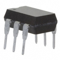
IL440
Vishay Semiconductors
Optocoupler, Phototriac Output, Low Input Current
A 1
6 MT2
C 2
5 NC
FEATURES
• 400 V blocking voltage
• 5 mA maximum trigger current
• Isolation test voltage, 5300 VRMS, t = 1 s
4 MT1
NC 3
• Isolation materials per UL94
i179035_2
• Pin compatible with optocouplers:
- IL440-4 MOC 3021
- IL440-5 MOC 3022
- IL440-6 MOC 3023
V
D E
i179035
DESCRIPTION
The IL440 consists of a GaAs infrared emitter optically
coupled to a silicon planar triac chip with a non-zero
crossing network. The two semiconductors are assembled
in a 6 pin dual-in-line plastic package. The IL440 can handle
currents up to 100 mA RMS.
• Compliant to RoHS Directive 2002/95/EC and in
accordance to WEEE 2002/96/EC
APPLICATIONS
• High current triac driver
AGENCY APPROVALS
• Solid state relay
• UL1577, file no. E52744 system code H or J, double
protection
• Switch small AC loads
• CSA 93751
• DIN EN 60747-5-5 (VDE 0884) available with option 1
• BSI IEC60950; IEC60065
ORDERING INFORMATION
I
L
4
4
0
-
PART NUMBER
#
TRIGGER
CURRENT
BIN
X
0
#
#
PACKAGE OPTION
DIP
Option 6
7.62 mm
10.16 mm
Option 7
Option 9
T
TAPE AND
REEL
> 0.1 mm
> 0.7 mm
AGENCY CERTIFIED/PACKAGE
TRIGGER CURRENT, IFT
UL, cUL, BSI
DIP-6
5 mA
10 mA
15 mA
IL440-6
IL440-5
IL440-4
SMD-6, option 7
IL440-6X007
-
-
SMD-6, option 9
IL440-6X009T (1)
IL440-5X009
IL440-4X009T (1)
15 mA
VDE, UL, cUL, BSI
5 mA
10 mA
IL440-6X016
IL440-5X016
-
SMD-6, option 7
-
IL440-5X017T
IL440-4X017
SMD-6, option 9
IL440-6X019T
-
-
DIP-6, 400 mil, option 6
Note
(1) Also available in tubes, do not put T on the end.
Document Number: 83631
Rev. 1.9, 29-Oct-10
For technical questions, contact: optocoupleranswers@vishay.com
www.vishay.com
1
�IL440
Vishay Semiconductors Optocoupler, Phototriac Output, Low
Input Current
ABSOLUTE MAXIMUM RATINGS (1) (Tamb = 25 °C, unless otherwise specified)
PARAMETER
TEST CONDITION
PART
SYMBOL
VALUE
UNIT
VR
IF
5
60
3
100
100
V
mA
A
mW
°C
ID(RMS)
IFSM
IDRM
Pdiss
Tj
400
400
400
100
1.2
2
300
125
V
V
V
mA
A
A
mW
°C
VISO
Input
Reverse voltage
Forward current
Surge current
Power dissipation
Junction temperature
Output
P.W. < 10 μs
IL440-4
IL440-5
IL440-6
Peak off-state voltage
On-state RMS current
Peak surge current
Peak on-state current
Power dissipation
Junction temperature
Coupler
IFSM
Pdiss
Tj
tp ≤ 10 ms
tp/T = 0.01 ≤ 100 μs
VDRM
VDRM
VDRM
5300
VRMS
Creepage distance
≥7
mm
Clearance distance
≥7
mm
Ω
Isolation voltage
t=1s
VIO = 500 V, Tamb = 25 °C
RIO
≥ 1012
VIO = 500 V, Tamb = 100 °C
RIO
≥ 1011
Ω
Ptot
330
mW
Storage temperature range
Tstg
- 55 to + 125
°C
Ambient temperature
Tamb
- 40 to + 100
°C
Junction temperature
Tj
100
°C
Tsld
260
°C
Isolation resistance
Total power dissipation
Lead soldering temperature (2)
2 mm from case, t < 10 s
Notes
(1) Stresses in excess of the absolute maximum ratings can cause permanent damage to the device. Functional operation of the device is not
implied at these or any other conditions in excess of those given in the operational sections of this document. Exposure to absolute
maximum ratings for extended periods of the time can adversely affect reliability.
(2) Refer to reflow profile for soldering conditions for surface mounted devices (SMD). Refer to wave profile for soldering conditions for through
hole devices (DIP).
www.vishay.com
2
For technical questions, contact: optocoupleranswers@vishay.com
Document Number: 83631
Rev. 1.9, 29-Oct-10
�IL440
Optocoupler, Phototriac Output, Low Vishay Semiconductors
Input Current
ELECTRICAL CHARACTERISTICS (1) (Tamb = 25 °C, unless otherwise specified)
PARAMETER
TEST CONDITION
PART
SYMBOL
MIN.
TYP.
MAX.
UNIT
Input
Forward voltage
IF = 50 mA
VF
Reverse voltage
IR = 10 μA
VR
VR = 0 V, f = 1 MHz
Cj
Junction capacitance
1.25
V
5
V
50
pF
Output (2)
IL440-4
Off-state voltage
IDRM = 500 nA
IL440-5
VD(RMS)
IL440-6
ITM = 100 mA, IFT = 30 mA
Peak on-state voltage
Trigger current 1
VT = 6 V, RL = 150 Ω
Trigger current 2
Trigger current 3
400
V
400
V
400
V
VTM
1.5
3
V
IL440-4
IFT1
15
IL440-5
IFT2
10
V
IL440-6
IFT3
5
V
50
V/μs
0.25
V/μs
1
mA
Critical rate of rise of off-state voltage
IF = 0, VD = 0.67 VDRM
dV/dtcr
Critical rate of rise of on-state current
commutation
IF = 30 mA, VD = 60 VRMS
dV/dtcrq
IF ≥ 10 mA, VS ≥ 3 V
IH
0.13
V
Coupler
Holding current
Notes
(1) Minimum and maximum values are testing requirements. Typical values are characteristics of the device and are the result of engineering
evaluation. Typical values are for information only and are not part of the testing requirements.
(2) Off-state output terminal voltage (see table 1.)
MAXIMUM SAFETY RATINGS (1)
PARAMETER
TEST CONDITION
SYMBOL
MIN.
TYP.
MAX.
UNIT
IS, INPUT
130
mA
PS, OUTPUT
300
mW
INPUT (2)
Forward voltage
OUTPUT
Power dissipation
Notes
(1) According to DIN EN 60747-5-5. This optocoupler is suitable for safe electrical isolation only within the safety ratings. Compliance with the
safety ratings shall be ensured by means of suitable protective circuits.
(2) The device is used for protective separation agains electrical shock within the maximum safety ratings. This must be ensured by protective
circuits in the applications.
SAFETY AND INSULATION RATINGS
PARAMETER
TEST CONDITION
SYMBOL
MIN.
Climatic classification
(according to IEC68 part 1)
Pollution degree
TYP.
MAX.
UNIT
55/100/21
DIN VDE 0109
Comparative tracking index
2
CTI
175
VIOTM
8000
Vpeak
VIORM
890
Vpeak
Insulation resistance at 25 °C
VIO = 500 V
RIS
≥ 1012
Ω
109
Ω
Insulation resistance at TS
VIO = 500 V
RIS
≥
Insulation resistance at 100 °C
VIO = 500 V
RIS
≥ 1011
Ω
Method a,
Vpd = VIORM x 1.875
Vpd
1669
Vpeak
PSO
500
mW
ISI
250
mA
TSI
175
°C
Partial discharge test voltage
Document Number: 83631
Rev. 1.9, 29-Oct-10
For technical questions, contact: optocoupleranswers@vishay.com
www.vishay.com
3
�IL440
Vishay Semiconductors Optocoupler, Phototriac Output, Low
Input Current
SAFETY AND INSULATION RATINGS
PARAMETER
TEST CONDITION
SYMBOL
MIN.
TYP.
MAX.
UNIT
Clearance distance
Standard DIP-6
7
mm
Creepage distance
Standard DIP-6
7
mm
Clearance distance
400 mil DIP-6
8
mm
Creepage distance
400 mil DIP-6
8
mm
Note
• As per IEC60747-5-5, § 7.4.3.8.1, this optocoupler is suitable for “safe electrical insulation” only within the safety ratings. Compliance with
the safety ratings shall be ensured by means of prodective circuits.
PACKAGE DIMENSIONS in millimeters
Pin one ID
3
2
1
4
5
6
6.4 ± 0.1
ISO method A
8.6 ± 0.1
7.62 typ.
0.5 ± 0.05
1 min.
3.555 ± 0.255
18°
4° typ.
2.95 ± 0.5
0.8 min.
0.85 ± 0.05
0.5 ± 0.05
3° to 9°
0.25 typ.
7.62 to 8.81
i178004
2.54 typ.
Option 6
Option 7
Option 9
10.36
9.96
7.62 typ.
9.53
10.03
7.8
7.4
7.62 ref.
0.7
4.6
4.1
0.102
0.249
8 min.
0.25 typ.
0.51
1.02
0.35
0.25
8.4 min.
15° max.
8 min.
10.16
10.92
10.3 max.
18450
PACKAGE MARKING
IL440
V YWW H 68
21764-91
www.vishay.com
4
For technical questions, contact: optocoupleranswers@vishay.com
Document Number: 83631
Rev. 1.9, 29-Oct-10
�DIP-6A
VISHAY
Vishay Semiconductors
DIP-6A
Package Dimensions in Inches (mm)
3
2
1
4
5
6
pin one ID
.248 (6.30)
.256 (6.50)
ISO Method A
.335 (8.50)
.343 (8.70)
.039
(1.00)
Min.
4°
typ.
.018 (0.45)
.022 (0.55)
.300 (7.62)
typ.
.048 (0.45)
.022 (0.55)
.130 (3.30)
.150 (3.81)
18°
.031 (0.80) min.
.031 (0.80)
.035 (0.90)
.100 (2.54) typ.
3°–9°
.114 (2.90)
.130 (3.0)
.010 (.25)
typ.
.300–.347
(7.62–8.81)
i178004
Document Number 83263
Rev. 1.1, 10-Dec-03
www.vishay.com
1
�DIP-6A
VISHAY
Vishay Semiconductors
Ozone Depleting Substances Policy Statement
It is the policy of Vishay Semiconductor GmbH to
1. Meet all present and future national and international statutory requirements.
2. Regularly and continuously improve the performance of our products, processes, distribution and
operatingsystems with respect to their impact on the health and safety of our employees and the public, as
well as their impact on the environment.
It is particular concern to control or eliminate releases of those substances into the atmosphere which are
known as ozone depleting substances (ODSs).
The Montreal Protocol (1987) and its London Amendments (1990) intend to severely restrict the use of ODSs
and forbid their use within the next ten years. Various national and international initiatives are pressing for an
earlier ban on these substances.
Vishay Semiconductor GmbH has been able to use its policy of continuous improvements to eliminate the
use of ODSs listed in the following documents.
1. Annex A, B and list of transitional substances of the Montreal Protocol and the London Amendments
respectively
2. Class I and II ozone depleting substances in the Clean Air Act Amendments of 1990 by the Environmental
Protection Agency (EPA) in the USA
3. Council Decision 88/540/EEC and 91/690/EEC Annex A, B and C (transitional substances) respectively.
Vishay Semiconductor GmbH can certify that our semiconductors are not manufactured with ozone depleting
substances and do not contain such substances.
We reserve the right to make changes to improve technical design
and may do so without further notice.
Parameters can vary in different applications. All operating parameters must be validated for each
customer application by the customer. Should the buyer use Vishay Semiconductors products for any
unintended or unauthorized application, the buyer shall indemnify Vishay Semiconductors against all
claims, costs, damages, and expenses, arising out of, directly or indirectly, any claim of personal
damage, injury or death associated with such unintended or unauthorized use.
Vishay Semiconductor GmbH, P.O.B. 3535, D-74025 Heilbronn, Germany
Telephone: 49 (0)7131 67 2831, Fax number: 49 (0)7131 67 2423
www.vishay.com
2
Document Number 83263
Rev. 1.1, 10-Dec-03
�Footprints
Vishay Semiconductors
Footprints
0.004 (0.1)
0.398 (10.2)
5)
0.236 (5.99)
0.293 (7.5)
6 (0.1
R 0.010 (0.13)
0.050 (1.27)
0.00
0.027 (0.7)
0.045 (1.14)
0.260 (6.6)
17977
0.050 (1.27)
Fig. 1 - SO8A and DSO8A SMD
0.273 (7.0)
0.004 (0.1)
Possible footprint
0.325 (8.2)
0.035 (0.9)
0.036 (0.91)
0.170 (4.32)
0.099 (2.54)
0.014 (0.36)
0.425 (10.8)
0.172 (4.4)
18406
6 (0.
0.00
0.027 (0.7)
15)
Fig. 3 - SOP-6, 5 Pin Wide Body
Possible footprint
0.035 (0.9)
0.050 (1.27)
0.336 (8.53)
R 0.010 (0.25)
0.050 (1.27)
0.014 (0.36)
0.036 (0.91)
0.266 (6.76)
0.195 (5.0)
17972
0.045 (1.14)
0.356 (9.04)
0.296 (7.6)
18403
Fig. 2 - SOP-4, Miniflat
Document Number: 83715
Rev. 1.4, 11-Jan-08
Fig. 4 - 8 Pin PCMCIA
For technical questions, please contact: optocoupler.answers@vishay.com
www.vishay.com
1
�Footprints
Footprints
Vishay Semiconductors
0.336 (8.53)
R 0.010 (0.25)
0.270 (6.86)
R 0.010 (0.25)
0.014 (0.36)
0.086 (2.18)
0.050 (1.27)
0.014 (0.36)
0.100 (2.54)
0.036 (0.91)
0.200 (5.08)
0.036 (0.91)
0.266 (6.76)
0.045 (1.14)
0.045 (1.14)
0.290 (7.37)
17973
0.356 (9.04)
17976
Fig. 8 - 4 Pin Mini-Flat
Fig. 5 - 8 Pin PCMCIA, Heat Sink
0.398 (10.2)
0.004 (0.1)
0.293 (7.5)
0.276 (7.01)
6 (0.1
5)
0.010 (0.25)
0.027 (0.7)
R 0.005 (0.13)
0.040 (1.02)
17978
0.099 (2.54)
0.024 (0.61)
0.026 (0.66)
0.050 (1.27)
0.00
0.053 (1.35)
0.216 (5.49)
Possible footprint
0.296 (7.52)
Fig. 6 - Mini Coupler
0.325 (8.2)
0.035 (0.9)
0.425 (10.8)
18405
0.270 (6.86)
Fig. 9 - SOP-6, 4 Pin Wide Body
R 0.010 (0.25)
0.406 (10.31)
0.050 (1.27)
0.030 (0.76)
0.014 (0.36)
0.100 (2.54)
R 0.010 (0.25)
0.036 (0.91)
0.200 (5.08)
17974
0.290 (7.37)
Fig. 7 - SOP-16
www.vishay.com
2
0.070 (1.78)
0.315 (8.00) min.
0.045 (1.14)
1796 2
0.060 (1.52)
0.435 (11.05)
Fig. 10 - 4 Pin SMD Option 7
For technical questions, please contact: optocoupler.answers@vishay.com
Document Number: 83715
Rev. 1.4, 11-Jan-08
�Footprints
Footprints
Vishay Semiconductors
0.406 (10.31)
0.406 (10.31)
0.030 (0.76)
R 0.010 (0.25)
0.100 (2.54)
0.070 (1.78)
0.315 (8.00) min.
17963
0.060 (1.52)
0.435 (11.05)
Fig. 11 - 6 Pin SMD Option 7
0.030 (0.76)
0.100 (2.54)
R 0.010 (0.25)
0.070 (1.78)
0.315 (8.00) min.
0.406 (10.31)
17965
0.060 (1.52)
0.435 (11.05)
Fig. 13 - 16 Pin SMD Option 7
0.030 (0.76)
R 0.010 (0.25)
0.100 (2.54)
0.070 (1.78)
0.315 (8.00) min.
17964
0.472 (11.99)
0.060 (1.52)
0.435 (11.05)
0.030 (0.76)
Fig. 12 - 8 Pin SMD Option 7
R 0.010 (0.25)
0.100 (2.54)
0.070 (1.78)
0.392 (9.95) min.
17966
0.060 (1.52)
0.512 (13.00)
Fig. 14 - 4 Pin SMD Option 8
Document Number: 83715
Rev. 1.4, 11-Jan-08
For technical questions, please contact: optocoupler.answers@vishay.com
www.vishay.com
3
�Footprints
Footprints
Vishay Semiconductors
0.472 (11.99)
0.395 (10.03)
0.030 (0.76)
R 0.010 (0.25)
0.100 (2.54)
0.030 (0.76)
0.070 (1.78)
0.392 (9.95) min.
17967
0.060 (1.52)
R 0.010 (0.25)
0.100 (2.54)
0.512 (13.00)
0.070 (1.78)
0.315 (8.00) min.
Fig. 15 - 6 Pin SMD Option 8
17970
0.060 (1.52)
0.435 (11.05)
Fig. 18 - 8 Pin SMD Option 9
0.395 (10.03)
0.395 (10.03)
0.100 (2.54)
R 0.010 (0.25)
0.030 (0.76)
0.070 (1.78)
0.315 (8.00) min.
17968
0.060 (1.52)
0.435 (11.05)
Fig. 16 - 4 Pin SMD Option 9
0.030 (0.76)
0.395 (10.03)
0.030 (0.76)
0.100 (2.54)
R 0.010 (0.25)
0.070 (1.78)
0.100 (2.54)
0.315 (8.00) min.
R 0.010 (0.25)
17971
0.060 (1.52)
0.435 (11.05)
0.070 (1.78)
0.315 (8.00) min.
17969
0.435 (11.05)
0.060 (1.52)
Fig. 19 - 16 Pin SMD Option 9
Fig. 17 - 6 Pin SMD Option 9
www.vishay.com
4
For technical questions, please contact: optocoupler.answers@vishay.com
Document Number: 83715
Rev. 1.4, 11-Jan-08
�Footprints
Footprints
Vishay Semiconductors
0.336 (8.53)
R 0.010 (0.25)
0.050 (1.27)
0.100 (2.54)
0.014 (0.36)
0.036 (0.91)
0.266 (6.76)
17975
0.045(1.14)
0.356 (9.04)
Fig. 20 - 16 Pin PCMCIA
Document Number: 83715
Rev. 1.4, 11-Jan-08
For technical questions, please contact: optocoupler.answers@vishay.com
www.vishay.com
5
�Legal Disclaimer Notice
Vishay
Disclaimer
ALL PRODUCT, PRODUCT SPECIFICATIONS AND DATA ARE SUBJECT TO CHANGE WITHOUT NOTICE TO IMPROVE
RELIABILITY, FUNCTION OR DESIGN OR OTHERWISE.
Vishay Intertechnology, Inc., its affiliates, agents, and employees, and all persons acting on its or their behalf (collectively,
“Vishay”), disclaim any and all liability for any errors, inaccuracies or incompleteness contained in any datasheet or in any other
disclosure relating to any product.
Vishay makes no warranty, representation or guarantee regarding the suitability of the products for any particular purpose or
the continuing production of any product. To the maximum extent permitted by applicable law, Vishay disclaims (i) any and all
liability arising out of the application or use of any product, (ii) any and all liability, including without limitation special,
consequential or incidental damages, and (iii) any and all implied warranties, including warranties of fitness for particular
purpose, non-infringement and merchantability.
Statements regarding the suitability of products for certain types of applications are based on Vishay’s knowledge of typical
requirements that are often placed on Vishay products in generic applications. Such statements are not binding statements
about the suitability of products for a particular application. It is the customer’s responsibility to validate that a particular
product with the properties described in the product specification is suitable for use in a particular application. Parameters
provided in datasheets and/or specifications may vary in different applications and performance may vary over time. All
operating parameters, including typical parameters, must be validated for each customer application by the customer’s
technical experts. Product specifications do not expand or otherwise modify Vishay’s terms and conditions of purchase,
including but not limited to the warranty expressed therein.
Except as expressly indicated in writing, Vishay products are not designed for use in medical, life-saving, or life-sustaining
applications or for any other application in which the failure of the Vishay product could result in personal injury or death.
Customers using or selling Vishay products not expressly indicated for use in such applications do so at their own risk and agree
to fully indemnify and hold Vishay and its distributors harmless from and against any and all claims, liabilities, expenses and
damages arising or resulting in connection with such use or sale, including attorneys fees, even if such claim alleges that Vishay
or its distributor was negligent regarding the design or manufacture of the part. Please contact authorized Vishay personnel to
obtain written terms and conditions regarding products designed for such applications.
No license, express or implied, by estoppel or otherwise, to any intellectual property rights is granted by this document or by
any conduct of Vishay. Product names and markings noted herein may be trademarks of their respective owners.
Document Number: 91000
Revision: 11-Mar-11
www.vishay.com
1
�