查询"IRFPS40N50LPBF"供应商
PD- 95141
IRFPS40N50LPbF
SMPS MOSFET
®
HEXFET Power MOSFET
Applications
• Zero Voltage Switching SMPS
VDSS RDS(on) typ. Trr typ. ID
• Telecom and Server Power Supplies
500V
170ns 46A
0.087Ω
• Uninterruptible Power Supplies
• Motor Control applications
• Lead-Free
Features and Benefits
• SuperFast body diode eliminates the need for external
diodes in ZVS applications.
• Lower Gate charge results in simpler drive requirements.
• Enhanced dv/dt capabilities offer improved ruggedness.
• Higher Gate voltage threshold offers improved noise
Super-247™
immunity.
Absolute Maximum Ratings
Parameter
ID @ TC = 25°C Continuous Drain Current, VGS @ 10V
Max.
ID @ TC = 100°C Continuous Drain Current, VGS @ 10V
29
IDM
180
Pulsed Drain Current
PD @TC = 25°C Power Dissipation
c
VGS
Linear Derating Factor
Gate-to-Source Voltage
dv/dt
TJ
Peak Diode Recovery dv/dt
Operating Junction and
TSTG
Storage Temperature Range
Units
46
d
A
540
W
4.3
±30
W/°C
V
34
-55 to + 150
V/ns
°C
Soldering Temperature, for 10 seconds
300 (1.6mm from case )
Diode Characteristics
Symbol
Parameter
Min. Typ. Max. Units
IS
Continuous Source Current
–––
–––
46
ISM
(Body Diode)
Pulsed Source Current
–––
–––
180
–––
–––
1.5
V
ns
�c
A
(Body Diode)
VSD
Diode Forward Voltage
trr
Reverse Recovery Time
Qrr
Reverse Recovery Charge
IRRM
Reverse Recovery Current
ton
Forward Turn-On Time
www.irf.com
Conditions
MOSFET symbol
showing the
integral reverse
p-n junction diode.
TJ = 25°C, IS = 46A, VGS = 0V
TJ = 25°C, IF = 46A
–––
170
250
–––
220
330
–––
705
1060
–––
1.3
2.0
nC TJ = 25°C, IS = 46A, VGS = 0V
TJ = 125°C, di/dt = 100A/µs
–––
9.0
–––
A
TJ = 125°C, di/dt = 100A/µs
f
f
f
f
TJ = 25°C
Intrinsic turn-on time is negligible (turn-on is dominated by LS+LD)
1
09/14/04
�查询"IRFPS40N50LPBF"供应商
IRFPS40N50LPbF
Static @ TJ = 25°C (unless otherwise specified)
Symbol
Parameter
V(BR)DSS
Drain-to-Source Breakdown Voltage
500
∆V(BR)DSS/∆TJ
Breakdown Voltage Temp. Coefficient
RDS(on)
Static Drain-to-Source On-Resistance
VGS(th)
Gate Threshold Voltage
3.0
IDSS
Drain-to-Source Leakage Current
IGSS
RG
Min. Typ. Max. Units
Conditions
–––
–––
V
VGS = 0V, ID = 250µA
–––
0.60
–––
V/°C
Reference to 25°C, ID = 1mA
–––
0.087 0.100
–––
5.0
Ω
V
VGS = 10V, ID = 28A
f
VDS = VGS, ID = 250µA
–––
–––
50
µA
VDS = 500V, VGS = 0V
–––
–––
2.0
mA
VDS = 400V, VGS = 0V, TJ = 125°C
nA
Gate-to-Source Forward Leakage
–––
–––
100
Gate-to-Source Reverse Leakage
–––
–––
-100
Internal Gate Resistance
–––
0.90
–––
VGS = 30V
VGS = -30V
Ω
f = 1MHz, open drain
Dynamic @ TJ = 25°C (unless otherwise specified)
Symbol
Parameter
gfs
Qg
Forward Transconductance
Min. Typ. Max. Units
Total Gate Charge
Qgs
Gate-to-Source Charge
Qgd
Gate-to-Drain ("Miller") Charge
–––
–––
190
td(on)
Turn-On Delay Time
–––
27
–––
tr
Rise Time
–––
170
–––
td(off)
Turn-Off Delay Time
–––
50
–––
tf
Fall Time
–––
69
–––
Ciss
Input Capacitance
–––
8110
–––
Coss
Output Capacitance
–––
960
–––
VDS = 25V
Crss
Reverse Transfer Capacitance
–––
130
–––
Coss
Output Capacitance
–––
11200
–––
ƒ = 1.0MHz, See Fig. 5
VGS = 0V, VDS = 1.0V, ƒ = 1.0MHz
Coss
Output Capacitance
–––
240
–––
Coss eff.
Effective Output Capacitance
–––
440
–––
Coss eff. (ER)
Effective Output Capacitance
–––
310
–––
21
–––
–––
–––
–––
380
–––
–––
80
Conditions
S
VDS = 50V, ID = 46A
nC
VDS = 400V
ID = 46A
VGS = 10V, See Fig. 7 & 15
f
VDD = 250V
ns
ID = 46A
RG = 0.85Ω
VGS = 10V, See Fig. 14a & 14b
f
VGS = 0V
pF
VGS = 0V, VDS = 400V, ƒ = 1.0MHz
VGS = 0V,VDS = 0V to 400V
g
(Energy Related)
Avalanche Characteristics
Symbol
EAS
IAR
EAR
Parameter
Single Pulse Avalanche Energy
Avalanche Current
�c
Repetitive Avalanche Energy
d
c
Typ.
–––
Max.
920
Units
mJ
–––
46
A
–––
54
mJ
Typ.
Max.
Units
–––
0.23
0.24
–––
–––
40
Thermal Resistance
Symbol
RθJC
RθCS
RθJA
Parameter
Junction-to-Case
h
Case-to-Sink, Flat, Greased Surface
Junction-to-Ambient
h
Notes:
Repetitive rating; pulse width limited by
max. junction temperature. (See Fig. 11).
Starting TJ = 25°C, L = 0.86mH, RG = 25Ω,
IAS = 46A. (See Figure 12).
ISD ≤ 46A, di/dt ≤ 550A/µs, VDD ≤ V(BR)DSS,
TJ ≤ 150°C.
2
°C/W
Pulse width ≤ 400µs; duty cycle ≤ 2%.
Coss eff. is a fixed capacitance that gives the same charging time
as Coss while VDS is rising from 0 to 80% VDSS.
Coss eff.(ER) is a fixed capacitance that stores the same energy
as Coss while VDS is rising from 0 to 80% VDSS.
Rθ is measured at TJ approximately 90°C
www.irf.com
�查询"IRFPS40N50LPBF"供应商
IRFPS40N50LPbF
1000
VGS
15V
10V
8.0V
7.0V
6.0V
5.5V
5.0V
BOTTOM 4.5V
TOP
100
100
10
1
4.5V
0.1
20µs PULSE WIDTH
TJ = 25 °C
0.01
0.1
1
10
10
100
RDS(on) , Drain-to-Source On Resistance
(Normalized)
I D , Drain-to-Source Current (A)
10
TJ = 25 ° C
1
V DS= 50V
20µs PULSE WIDTH
6
7
8
9
10
VGS , Gate-to-Source Voltage (V)
Fig 3. Typical Transfer Characteristics
www.irf.com
10
100
Fig 2. Typical Output Characteristics
TJ = 150° C
5
1
VDS , Drain-to-Source Voltage (V)
1000
4
20µs PULSE WIDTH
TJ = 150 °C
0.1
0.1
Fig 1. Typical Output Characteristics
0.1
4.5V
1
VDS , Drain-to-Source Voltage (V)
100
VGS
15V
10V
8.0V
7.0V
6.0V
5.5V
5.0V
BOTTOM4.5V
TOP
I D , Drain-to-Source Current (A)
I D , Drain-to-Source Current (A)
1000
11
3.0
ID = 47A
2.5
2.0
1.5
1.0
0.5
0.0
-60 -40 -20
VGS = 10V
0
20 40 60
80 100 120 140 160
TJ , Junction Temperature ( ° C)
Fig 4. Normalized On-Resistance
vs. Temperature
3
�查询"IRFPS40N50LPBF"供应商
IRFPS40N50LPbF
1000000
100000
35
Coss = Cds + Cgd
10000
30
Energy (µJ)
C, Capacitance(pF)
40
VGS = 0V, f = 1 MHZ
Ciss = Cgs + Cgd, Cds SHORTED
Crss = Cgd
Ciss
1000
Coss
100
25
20
15
10
Crss
5
10
1
10
100
0
1000
0
VDS, Drain-to-Source Voltage (V)
V DS= 400V
V DS= 250V
V DS= 100V
15
ISD , Reverse Drain Current (A)
VGS , Gate-to-Source Voltage (V)
400
500
600
1000
100
10
5
0
100
200
300
QG , Total Gate Charge (nC)
Fig 7. Typical Gate Charge vs.
Gate-to-Source Voltage
4
300
Fig 6. Typ. Output Capacitance
Stored Energy vs. VDS
ID = 47A
0
200
VDS, Drain-to-Source Voltage (V)
Fig 5. Typical Capacitance vs.
Drain-to-Source Voltage
20
100
400
TJ = 150° C
10
TJ = 25 ° C
1
0.1
0.2
V GS = 0 V
0.7
1.2
1.7
2.2
VSD ,Source-to-Drain Voltage (V)
Fig 8. Typical Source-Drain Diode
Forward Voltage
www.irf.com
�查询"IRFPS40N50LPBF"供应商
IRFPS40N50LPbF
50
VGS
40
ID , Drain Current (A)
RD
V DS
RG
30
D.U.T.
+
-VDD
10V
Pulse Width ≤ 1 µs
Duty Factor ≤ 0.1 %
20
Fig 10a. Switching Time Test Circuit
10
VDS
90%
0
25
50
75
100
125
150
TC , Case Temperature ( °C)
10%
VGS
Fig 9. Maximum Drain Current vs.
Case Temperature
td(on)
tr
t d(off)
tf
Fig 10b. Switching Time Waveforms
Thermal Response(Z thJC )
1
0.1
D = 0.50
0.20
0.10
0.05
0.01
0.02
0.01
0.001
0.00001
PDM
t1
SINGLE PULSE
(THERMAL RESPONSE)
t2
Notes:
1. Duty factor D = t 1 / t 2
2. Peak TJ = P DM x Z thJC + TC
0.0001
0.001
0.01
0.1
1
t1 , Rectangular Pulse Duration (sec)
Fig 11. Maximum Effective Transient Thermal Impedance, Junction-to-Case
www.irf.com
5
�查询"IRFPS40N50LPBF"供应商
IRFPS40N50LPbF
1000
ID , Drain Current (A)
EAS , Single Pulse Avalanche Energy (mJ)
2000
OPERATION IN THIS AREA LIMITED
BY RDS(on)
TOP
BOTTOM
ID
21A
30A
46A
1500
100
10us
100us
10
1
1000
1ms
TC = 25 °C
TJ = 150 °C
Single Pulse
10ms
10
100
1000
VDS , Drain-to-Source Voltage (V)
500
0
25
50
75
100
125
150
Starting TJ , Junction Temperature( ° C)
Fig 13. Maximum Avalanche Energy
vs. Drain Current
Fig 12. Maximum Safe Operating
Area
15V
V(BR)DSS
DRIVER
L
VDS
D.U.T
RG
+
V
- DD
IAS
20V
0.01Ω
tp
tp
A
I AS
Fig 14a. Unclamped Inductive Test Circuit
Fig 14b. Unclamped Inductive Waveforms
Current Regulator
Same Type as D.U.T.
QG
50KΩ
12V
VGS
.2µF
.3µF
D.U.T.
QGS
+
V
- DS
QGD
VG
VGS
3mA
IG
ID
Current Sampling Resistors
Fig 15a. Gate Charge Test Circuit
6
Charge
Fig 15b. Basic Gate Charge Waveform
www.irf.com
�查询"IRFPS40N50LPBF"供应商
IRFPS40N50LPbF
Peak Diode Recovery dv/dt Test Circuit
Circuit Layout Considerations
• Low Stray Inductance
• Ground Plane
• Low Leakage Inductance
Current Transformer
+
D.U.T
+
-
-
+
RG
•
•
•
•
dv/dt controlled by RG
Driver same type as D.U.T.
ISD controlled by Duty Factor "D"
D.U.T. - Device Under Test
Driver Gate Drive
P.W.
Period
D=
+
-
V DD
P.W.
Period
VGS=10V
*
D.U.T. ISD Waveform
Reverse
Recovery
Current
Body Diode Forward
Current
di/dt
D.U.T. VDS Waveform
Diode Recovery
dv/dt
Re-Applied
Voltage
Body Diode
VDD
Forward Drop
Inductor Curent
Ripple ≤ 5%
ISD
* VGS = 5V for Logic Level Devices
Fig 16. For N-Channel HEXFET® Power MOSFETs
www.irf.com
7
�查询"IRFPS40N50LPBF"供应商
IRFPS40N50LPbF
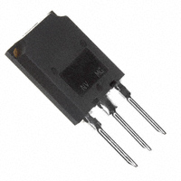
Case Outline and Dimensions — Super-247
Super-247 (TO-274AA) Part Marking Information
EXAMPLE: THIS IS AN IRFPS37N50A WITH
ASSEMBLY LOT CODE 1789
ASSEMBLED ON WW 19, 1997
IN THE ASSEMBLY LINE "C"
PART NUMBER
INTERNATIONAL RECTIFIER
LOGO
IRFPS37N50A
719C
17
89
ASSEMBLY LOT CODE
Note: "P" in assembly line position
indicates "Lead-Free"
DATE CODE
YEAR 7 = 1997
WEEK 19
LINE C
TOP
Data and specifications subject to change without notice.
This product has been designed and qualified for the industrial market.
Qualification Standards can be found on IR’s Web site.
IR WORLD HEADQUARTERS: 233 Kansas St., El Segundo, California 90245, USA Tel: (310) 252-7105
TAC Fax: (310) 252-7903
Visit us at www.irf.com for sales contact information.09/04
8
www.irf.com
�