L
www.vishay.com
Vishay Sfernice
SMD Wraparound Ultra Low Value Thin Film Resistors
FEATURES
• NiCr + Ta2O5 resistive layer
• Pre-soldered or gold terminations
• No inductance for high frequency applications
Available
• Alumina substrates for high power handling
capability
Available
• Resistance range: 0.1 to 9.99
• TCR down to 50 ppm/°C
Available
• Power rating: up to 2 W at +70 °C
• Withstand AEC-Q200 humidity test
ADDITIONAL RESOURCES
• Material categorization: for definitions of compliance
please see www.vishay.com/doc?99912
3D 3D
3D Models
Note
* This datasheet provides information about parts that are
RoHS-compliant and / or parts that are non RoHS-compliant. For
example, parts with lead (Pb) terminations are not RoHS-compliant.
Please see the information / tables in this datasheet for details
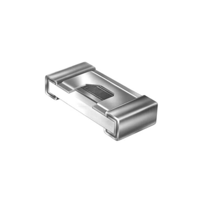
With extremely low resistance and high power capabilities,
these ultra low value resistors are available with solderable
or weldable terminations.
STANDARD ELECTRICAL SPECIFICATIONS
MODEL
SIZE
RESISTANCE RANGE
RATED POWER
P70 °C
W
LIMITING ELEMENT
VOLTAGE
V
TOLERANCE
±%
TEMPERATURE
COEFFICIENT
± ppm/°C
L0603
0603
0.1 to 9.99
0.125
50
1, 2, 3, 5, 10
50, 100, 200, 300
L0805
0805
0.1 to 9.99
0.2
50
1, 2, 3, 5, 10
50, 100, 200, 300
L1206
1206
0.1 to 9.99
0.33
50
1, 2, 3, 5, 10
50, 100, 200, 300
L1505
1505
0.1 to 9.99
0.5
50
1, 2, 3, 5, 10
50, 100, 200, 300
L2010
2010
0.1 to 9.99
1.0
50
1, 2, 3, 5, 10
50, 100, 200, 300
L2512
2512
0.1 to 9.99
2.0 (1)
50
1, 2, 3, 5, 10
50, 100, 200, 300
Note
(1) With special assembly care
CLIMATIC SPECIFICATIONS
TOLERANCE AND TCR VS. OHMIC VALUE
Operating temperature
range
TIGHTEST
BEST
OHMIC VALUE
TOLERANCE
TCR
RANGE in
(%)
(ppm/°C)
-55 °C; +155 °C
0R1 < 0R25
TERMINATIONS
1
300
N or B
0R25 < 0R5
1
200
N or B
0R5 < 2R5
1
100
N or B
1
50
N or B
5
300
G
MECHANICAL SPECIFICATIONS
Substrate
Alumina
NiCr + Ta2O5
2R5 < 9R99
Silicone
0R1 < 0R25
Solderable
B type: SnPb over nickel barrier
N type: SnAg over nickel barrier
G type: Gold over nickel barrier
0R25 < 0R5
5
200
G
0R < 1R
5
100
G
1R < 2R5
3
100
G
2R5 to 9R99
3
50
G
Technology
Coating
Terminations
Note
• Refer to Application Note “Guidelines for Vishay Sfernice
Resistive and Inductive Components” (document number:
52029) for recommended reflow profile. Profile #3 applies
Revision: 31-Jan-2020
Document Number: 53018
1
For technical questions, contact: sferthinfilm@vishay.com
THIS DOCUMENT IS SUBJECT TO CHANGE WITHOUT NOTICE. THE PRODUCTS DESCRIBED HEREIN AND THIS DOCUMENT
ARE SUBJECT TO SPECIFIC DISCLAIMERS, SET FORTH AT www.vishay.com/doc?91000
�L
www.vishay.com
Vishay Sfernice
DIMENSIONS in millimeters (inches)
A
B
C
D
E
A
B
C
D/E
± 0.152 (± 0.006)
± 0.127 (± 0.005)
± 0.127 (+ 0.005)
± 0.127 (± 0.005)
0603
1.52 (0.060)
0.85 (0.033)
0805
1.91 (0.075)
1.27 (0.050)
1206
3.06 (0.120)
1.60 (0.063)
CASE SIZE
0.38 (0.015)
0.40 (0.016)
0.5 (0.020)
1505
3.81 (0.150)
1.32 (0.052)
2010
5.08 (0.200)
2.54 (0.100)
2512
6.30 (0.248)
3.30 (0.129)
0.48 (0.019)
SUGGESTED LAND PATTERN in millimeters (inches) (to IPC-7351A)
Gmin.
Xmax.
Zmax.
CASE SIZE
Zmax.
Gmin.
Xmax.
0603
2.37 (0.093)
0.35 (0.014)
0.98 (0.039)
0805
2.76 (0.109)
0.74 (0.029)
1.40 (0.055)
1206
3.91 (0.154)
1.85 (0.073)
1.73 (0.068)
1505
4.66 (0.183)
2.44 (0.096)
1.45 (0.057)
2010
5.93 (0.233)
3.71 (0.146)
2.67 (0.105)
2512
7.15 (0.281)
4.93 (0.194)
3.43 (0.135)
Option: Enlarged Terminations: 0063
For stringent and special power dissipation requirements, the thermal resistance between the resistive layer and the solder joint
can be reduced using enlarged terminations chip resistors which are soldered on large and thick copper pads acting as heat
sinks (see application note: “Power Dissipation in High Precision Vishay Sfernice Chip Resistors and Arrays (P Thin Film, PRA
Arrays, CHP Thick Film)”: www.vishay.com/doc?53048).
For enlarged terminations: Please consult Vishay Sfernice.
Revision: 31-Jan-2020
Document Number: 53018
2
For technical questions, contact: sferthinfilm@vishay.com
THIS DOCUMENT IS SUBJECT TO CHANGE WITHOUT NOTICE. THE PRODUCTS DESCRIBED HEREIN AND THIS DOCUMENT
ARE SUBJECT TO SPECIFIC DISCLAIMERS, SET FORTH AT www.vishay.com/doc?91000
�L
www.vishay.com
Vishay Sfernice
Rated Power (%)
POWER DERATING CURVE
PACKAGING
Several types of packaging are proposed: waffle-pack and
tape and reel
100
NUMBER OF PIECES
PER PACKAGE
80
SIZE
MOQ
60
WAFFLE PACK
2" × 2"
0603
40
0
1206
1505
0
20
40
60 70 80
100
120
140 155
Ambient Temperature in °C
MIN.
140
100
TAPE
WIDTH
MAX.
5000
100
0805
20
TAPE AND REEL
100
4000
8 mm
60
2010
2512
2000
50
PACKAGING RULES
Waffle Pack
Can be filled up to maximum quantity indicated in the table
here above, taking into account the minimum order quantity.
When quantity ordered exceeds maximum quantity of a
single waffle pack, the waffle packs are stacked up on the
top of each other and closed by one single cover.
To get “not stacked up” waffle pack in case of ordered
quantity > maximum number of pieces per package:
Please consult Vishay Sfernice for specific ordering
code.
Tape and Reel
Can be filled up to maximum quantity indicated in the table
here above, taking into account the minimum order quantity.
When quantity ordered is between the MOQ and the
maximum reel capacity, only one reel is provided.
When several reels are needed for ordered quantity
within MOQ and maximum reel capacity: Please consult
Vishay Sfernice for specific ordering code.
PERFORMANCE
VALUES AND DRIFT
TESTS
Thermal shock
Short time overload
Low temperature operation
Resistance to solder heat
Moisture resistance
High temperature
Load life
Revision: 31-Jan-2020
CONDITIONS
MIL-R-55342
REQUIREMENTS
TYPICAL
PERFORMANCES
MIL-R-55342 C
MIL-STD-702, method 107
± 0.25 %
± 0.02 %
MIL-R-55342 C
PARA 3.10.4.7.5
± 0.10 %
± 0.01 %
MIL-R-55342 C
PARA 3.9 and 4.7.4
± 0.25 %
± 0.01 %
MIL-R-55342 C
PARA 3.12, 4.7.7, 4.7.1.2
± 0.25 %
± 0.04 %
MIL-R-55342 C
PARA 3.13 and 4.7.8
MIL-STD-202, method 106
± 0.40 %
± 0.01 %
AEC-Q200
85 °C / 85 % RH / 0.1 Pn
1000 h
-
Max. < 0.5 % + 0.05
MIL-R-55342 C
PARA 3.11 and 4.7.6
± 0.20 %
± 0.075 %
MIL-R-55342 C
2000 h Pn at 70 °C
MIL-STD-202, method 108
± 0.50 %
± 0.15 %
Document Number: 53018
3
For technical questions, contact: sferthinfilm@vishay.com
THIS DOCUMENT IS SUBJECT TO CHANGE WITHOUT NOTICE. THE PRODUCTS DESCRIBED HEREIN AND THIS DOCUMENT
ARE SUBJECT TO SPECIFIC DISCLAIMERS, SET FORTH AT www.vishay.com/doc?91000
�L
www.vishay.com
Vishay Sfernice
GLOBAL PART NUMBER INFORMATION
New Global Part Numbering: L0805K1R00FBT0099
L
0
GLOBAL
MODEL
L
8
0
5
K
1
R
0
0
F
B
T
0
0
9
9
SIZE
TCR
VALUE
TOLERANCE
TERMINATION (1)
PACKAGING
OPTION
0603
0805
1206
1505
2010
2512
H = ± 50 ppm
K = ± 100 ppm
L = ± 200 ppm
M = ± 300 ppm
R designated
decimal point
For values under 1R
Rxxx
F=±1%
G=±2%
H=±3%
J=±5%
K = ± 10 %
B: SnPb over
nickel barrier
N: SnAg over
nickel barrier
G: gold over
nickel barrier
For more
information see
Codification of
Packaging
table
Leave
blank if
no
option
Historical Part Number Example: L 0805 K 1R00 1 % B T R0099
L
0805
K
1R00
1%
B
T
R0099
MODEL
SIZE
TCR
VALUE
TOLERANCE
TERMINATION
PACKAGING
OPTION
Note
(1) B: lead bearing version
N and G: lead (Pb)-free / RoHS version
CODIFICATION OF PACKAGING
CODE 18
PACKAGING
WAFFLE PACK
W
100 min., 1 mult.
WA
100 min., 100 mult. (available only in size 1206)
PLASTIC TAPE (Standard for all sizes)
T
100 min., 1 mult.
TA
100 min., 100 mult.
TB
250 min., 250 mult.
TC
500 min., 500 mult.
TD
1000 min., 1000 mult.
TE
2500 min., 2500 mult.
TF
Full tape (quantity depending on size of chips)
PAPER TAPE (Available for 0603, 0805, and 1206. Please consult Vishay Sfernice for other sizes)
PT
100 min., 1 mult.
PA
100 min., 100 mult.
PB
250 min., 250 mult.
PC
500 min., 500 mult.
PD
1000 min., 1000 mult.
PE
2500 min., 2500 mult.
PF
Full tape (quantity depending on size of chips)
Revision: 31-Jan-2020
Document Number: 53018
4
For technical questions, contact: sferthinfilm@vishay.com
THIS DOCUMENT IS SUBJECT TO CHANGE WITHOUT NOTICE. THE PRODUCTS DESCRIBED HEREIN AND THIS DOCUMENT
ARE SUBJECT TO SPECIFIC DISCLAIMERS, SET FORTH AT www.vishay.com/doc?91000
�Legal Disclaimer Notice
www.vishay.com
Vishay
Disclaimer
ALL PRODUCT, PRODUCT SPECIFICATIONS AND DATA ARE SUBJECT TO CHANGE WITHOUT NOTICE TO IMPROVE
RELIABILITY, FUNCTION OR DESIGN OR OTHERWISE.
Vishay Intertechnology, Inc., its affiliates, agents, and employees, and all persons acting on its or their behalf (collectively,
“Vishay”), disclaim any and all liability for any errors, inaccuracies or incompleteness contained in any datasheet or in any other
disclosure relating to any product.
Vishay makes no warranty, representation or guarantee regarding the suitability of the products for any particular purpose or
the continuing production of any product. To the maximum extent permitted by applicable law, Vishay disclaims (i) any and all
liability arising out of the application or use of any product, (ii) any and all liability, including without limitation special,
consequential or incidental damages, and (iii) any and all implied warranties, including warranties of fitness for particular
purpose, non-infringement and merchantability.
Statements regarding the suitability of products for certain types of applications are based on Vishay's knowledge of typical
requirements that are often placed on Vishay products in generic applications. Such statements are not binding statements
about the suitability of products for a particular application. It is the customer's responsibility to validate that a particular product
with the properties described in the product specification is suitable for use in a particular application. Parameters provided in
datasheets and / or specifications may vary in different applications and performance may vary over time. All operating
parameters, including typical parameters, must be validated for each customer application by the customer's technical experts.
Product specifications do not expand or otherwise modify Vishay's terms and conditions of purchase, including but not limited
to the warranty expressed therein.
Hyperlinks included in this datasheet may direct users to third-party websites. These links are provided as a convenience and
for informational purposes only. Inclusion of these hyperlinks does not constitute an endorsement or an approval by Vishay of
any of the products, services or opinions of the corporation, organization or individual associated with the third-party website.
Vishay disclaims any and all liability and bears no responsibility for the accuracy, legality or content of the third-party website
or for that of subsequent links.
Except as expressly indicated in writing, Vishay products are not designed for use in medical, life-saving, or life-sustaining
applications or for any other application in which the failure of the Vishay product could result in personal injury or death.
Customers using or selling Vishay products not expressly indicated for use in such applications do so at their own risk. Please
contact authorized Vishay personnel to obtain written terms and conditions regarding products designed for such applications.
No license, express or implied, by estoppel or otherwise, to any intellectual property rights is granted by this document or by
any conduct of Vishay. Product names and markings noted herein may be trademarks of their respective owners.
© 2021 VISHAY INTERTECHNOLOGY, INC. ALL RIGHTS RESERVED
Revision: 09-Jul-2021
1
Document Number: 91000
�