LH1546AEF, LH1546AEFTR, LH1546AEFT2
www.vishay.com
Vishay Semiconductors
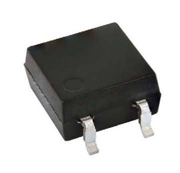
1 Form A Solid-State Relay (Normally Open)
FEATURES
• Current limit protection
S1
S2
A 1
4 S1
C 2
3
• Isolation test voltage 3750 VRMS
• Typical RON 22 Ω
• Load voltage 350 V
• Load current 120 mA
• High surge capability
S2
• Clean bounce free switching
• Low power consumption
• Material categorization: for definitions of compliance
please see www.vishay.com/doc?99912
DESCRIPTION
APPLICATIONS
The LH1546AEF (4 pin SOP) is robust, ideal for telecom and
ground fault applications. It is an SPST normally open
switch (1 Form A) that replaces electromechanical relays in
many applications. It is constructed using a GaAlAs LED for
actuation control and MOSFETs for the switch output. In
addition, it employs current-limiting circuitry to provide
overvoltage protection.
• General telecom switching
• Instrumentation
• Industrial controls
AGENCY APPROVALS
• UL1577, file no. E52744
ORDERING INFORMATION
L
H
1
5
PART NUMBER
PACKAGE
4
6
A
ELECTR.
VARIATION
#
#
PACKAGE
CONFIG.
T
R
SOP-4
TAPE AND
REEL
UL
SOP-4, tape and reel
LH1546AEFTR
SOP-4, tape and reel (T2 rotation)
LH1546AEFT2
SOP-4, tubes
Rev. 2.0, 11-Jul-2018
LH1546AEF
Document Number: 83837
1
For technical questions, contact: optocoupleranswers@vishay.com
THIS DOCUMENT IS SUBJECT TO CHANGE WITHOUT NOTICE. THE PRODUCTS DESCRIBED HEREIN AND THIS DOCUMENT
ARE SUBJECT TO SPECIFIC DISCLAIMERS, SET FORTH AT www.vishay.com/doc?91000
�LH1546AEF, LH1546AEFTR, LH1546AEFT2
www.vishay.com
Vishay Semiconductors
ABSOLUTE MAXIMUM RATINGS (Tamb = 25 °C, unless otherwise specified)
PARAMETER
CONDITIONS
SYMBOL
VALUE
UNIT
IRED continuous forward current
IF
50
mA
IRED reverse voltage
VR
5
V
Pdiss
80
mW
DC or peak AC load voltage
VL
350
V
Continuous DC load current
IL
120
mA
Pdiss
550
mW
INPUT
Input power dissipation
OUTPUT
SSR output power dissipation
SSR
Ambient temperature range
Tamb
-40 to +85
°C
Storage temperature range
Tstg
-40 to +150
°C
Tsld
260
°C
Soldering temperature
t = 10 s max.
Note
• Stresses in excess of the absolute maximum ratings can cause permanent damage to the device. Functional operation of the device is not
implied at these or any other conditions in excess of those given in the operational sections of this document. Exposure to absolute
maximum ratings for extended periods of the time can adversely affect reliability
ELECTRICAL CHARACTERISTICS (Tamb = 25 °C, unless otherwise specified)
PARAMETER
TEST CONDITION
SYMBOL
MIN.
TYP.
MAX.
UNIT
IRED forward current, switch turn-on
IL = 100 mA, t = 10 ms
IFon
-
0.3
2
mA
IRED forward current, switch turn-off
VL = ± 350 V, IL < 1 μA
IFoff
0.05
0.2
-
mA
IF = 10 mA
VF
1
1.36
1.45
V
INPUT
IRED forward voltage
OUTPUT
On-resistance
IF = 5 mA, IL = 50 mA
RON
-
22
27
Ω
Off-resistance
IF = 0 mA, VL = ± 100 V
ROFF
0.5
850
-
GΩ
Off-state leakage current
Output capacitance
Current limit AC/DC
IF = 0 mA, VL = ± 100 V
Ileak
-
5 mA
0
T = 25 °C
30
0
0
20
40
60
80
0
100
Tamb - Ambient Temperature (°C)
1.0
1.5
2.0
VF - Forward Voltage (V)
Fig. 4 - Maximum Load Current vs. Ambient Temperature
Fig. 6 - Forward Current vs. Forward Voltage
1.7
2.0
1.6
Normalized Turn-On Time
VF - Forward Voltage (V)
0.5
IF = 20 mA
1.5
IF = 10 mA
1.4
1.3
1.2
IF = 2 mA
IF = 5 mA
1.1
1.0
IF = 5 mA
1.5
1.0
0.5
Normalized to Tamb = 25 °C
0
-40
-20
0
20
40
60
80
Tamb - Ambient Temperature (°C)
Fig. 5 - Forward Voltage vs. Ambient Temperature
Rev. 2.0, 11-Jul-2018
-40
-20
0
20
40
60
80
Tamb - Ambient Temperature (°C)
Fig. 7 - Normalized Forward Current for Switch Turn-On vs.
Ambient Temperature
Document Number: 83837
4
For technical questions, contact: optocoupleranswers@vishay.com
THIS DOCUMENT IS SUBJECT TO CHANGE WITHOUT NOTICE. THE PRODUCTS DESCRIBED HEREIN AND THIS DOCUMENT
ARE SUBJECT TO SPECIFIC DISCLAIMERS, SET FORTH AT www.vishay.com/doc?91000
�LH1546AEF, LH1546AEFTR, LH1546AEFT2
www.vishay.com
Vishay Semiconductors
0.5
IF = 5.0 mA
IL = 50 mA
1.2
0.4
1.0
0.8
0.6
0.4
0.3
T = 25 °C
0.2
T = -40 °C
0.1
0.2
Normalized to Tamb = 25 °C
0
0
0
-40
-20
0
20
40
60
20
30
40
50
IF - Forward Current (mA)
Fig. 8 - Normalized On-Resistance vs. Ambient Temperature
Fig. 11 - Turn-On Time vs. Forward Current
1.8
60
IF = 0 mA
f = 1 MHz
50
Normalized Turn-On Time
Switch Capacitance (pF)
10
80
Tamb - Ambient Temperature (°C)
40
30
20
10
IF = 5 mA
1.6
1.4
1.2
1.0
0.8
0.6
0.4
0.2
Normalized to Tamb = 25 °C
0
0
0
10
20
30
40
50
-40
60
Fig. 9 - Output Capacitance vs. Load Voltage
IF = 0 mA
20
40
60
80
IL = 50 mA
0.16
Turn-Off Time (ms)
T = 85 °C
1
0
Fig. 12 - Normalized Turn-On Time vs. Ambient Temperature
100
10
-20
Tamb - Ambient Temperature (°C)
Applied Voltage (V)
Off-State Leakage Current (nA)
IL = 50 mA
T = 85 °C
Turn-On Time (ms)
Normalized On-Resistance
1.4
T = 25 °C
0.1
T = 85 °C
0.12
T = 25 °C
0.08
0.04
T = -40 °C
T = -40 °C
0
0.01
0
100
200
300
400
VL - Load Voltage (V)
Fig. 10 - Off-State Leakage Current vs. Load Voltage
Rev. 2.0, 11-Jul-2018
0
10
20
30
40
50
IF - Forward Current (mA)
Fig. 13 - Turn-Off Time vs. Forward Current
Document Number: 83837
5
For technical questions, contact: optocoupleranswers@vishay.com
THIS DOCUMENT IS SUBJECT TO CHANGE WITHOUT NOTICE. THE PRODUCTS DESCRIBED HEREIN AND THIS DOCUMENT
ARE SUBJECT TO SPECIFIC DISCLAIMERS, SET FORTH AT www.vishay.com/doc?91000
�LH1546AEF, LH1546AEFTR, LH1546AEFT2
www.vishay.com
Vishay Semiconductors
Normalized Turn-Off Time
1.8
1.6
1.4
1.2
IF = 5 mA
1.0
0.8
0.6
0.4
0.2
Normalized to Tamb = 25 °C
0
-40
-20
0
20
40
60
80
Tamb - Ambient Temperature (°C)
Fig. 14 - Normalized Turn-Off Time vs. Ambient Temperature
PACKAGE DIMENSIONS (in millimeters)
6.95 ± 0.25
4.42 ± 0.25
4.57 ± 0.25
0.41 ± 0.10
2.54 nom.
0.20 ± 0.10
5.35 typ.
0.05 ± 0.05 2.12 ± 0.20
4.92 max.
5.0 min.
0.50 ± 0.15
Leads coplanarity 0.1 max.
4
3
Pin 1 I.D.
0.90
2.54
Recommended footprint
1.15
5.10
1
7.40
2
Fig. 15 - Package Drawing
Rev. 2.0, 11-Jul-2018
Document Number: 83837
6
For technical questions, contact: optocoupleranswers@vishay.com
THIS DOCUMENT IS SUBJECT TO CHANGE WITHOUT NOTICE. THE PRODUCTS DESCRIBED HEREIN AND THIS DOCUMENT
ARE SUBJECT TO SPECIFIC DISCLAIMERS, SET FORTH AT www.vishay.com/doc?91000
�LH1546AEF, LH1546AEFTR, LH1546AEFT2
www.vishay.com
Vishay Semiconductors
PACKAGE MARKING (example)
LH1546
V YWW
68
Fig. 16 - LH1546AEF
Note
• Tape and reel suffix (TR) is not part of the package marking
PACKAGING INFORMATION (in millimeters)
ESD sticker
Tape slot
in core
330
(13")
Regular, special
or bar code label
17999
Fig. 17 - Tape and Reel Shipping Medium
(EIA-481, revision A, and IEC 60286), 2000 units per reel
0.35 ± 0.05
2.0 ± 0.1
4.0 ± 0.1
1.5 min.
Pin 1
1.75 ± 0.1
5.5 ± 0.05
12.0 ± 0.3
CL
7.33 ± 0.1
2.36 ± 0.1
8.0 ± 0.1
4.72 ± 0.1
1.5 min.
2.66 ± 0.1
Fig. 18 - Tape and Reel Packing
Notes
• Cumulative tolerance of 10 sprocket holes is 0.20 mm
• Applicable orientation as below:
T=
T2 =
DEVICES PER REEL
TYPE
UNITS/REEL
SOP-4
2000
Rev. 2.0, 11-Jul-2018
Document Number: 83837
7
For technical questions, contact: optocoupleranswers@vishay.com
THIS DOCUMENT IS SUBJECT TO CHANGE WITHOUT NOTICE. THE PRODUCTS DESCRIBED HEREIN AND THIS DOCUMENT
ARE SUBJECT TO SPECIFIC DISCLAIMERS, SET FORTH AT www.vishay.com/doc?91000
�LH1546AEF, LH1546AEFTR, LH1546AEFT2
www.vishay.com
Vishay Semiconductors
SOLDER PROFILES
HANDLING AND STORAGE CONDITIONS
ESD level: HBM class 2
Axis Title
10000
300
Floor life: unlimited
Max. 260 °C
255 °C
240 °C
217 °C
Conditions: Tamb < 30 °C, RH < 60 %
245 °C
Moisture sensitivity level 1, according to J-STD-020
1000
200
Max. 30 s
1st line
2nd line
2nd line
Temperature (°C)
250
150
Max. 120 s
100
Max. 100 s
Max. ramp down 6 °C/s
100
Max. ramp up 3 °C/s
50
10
0
0
50
100
150
200
250
300
Time (s)
19841
Fig. 19 - Lead (Pb)-free Reflow Solder Profile
According to J-STD-020 for SMD Devices
Rev. 2.0, 11-Jul-2018
Document Number: 83837
8
For technical questions, contact: optocoupleranswers@vishay.com
THIS DOCUMENT IS SUBJECT TO CHANGE WITHOUT NOTICE. THE PRODUCTS DESCRIBED HEREIN AND THIS DOCUMENT
ARE SUBJECT TO SPECIFIC DISCLAIMERS, SET FORTH AT www.vishay.com/doc?91000
�Legal Disclaimer Notice
www.vishay.com
Vishay
Disclaimer
ALL PRODUCT, PRODUCT SPECIFICATIONS AND DATA ARE SUBJECT TO CHANGE WITHOUT NOTICE TO IMPROVE
RELIABILITY, FUNCTION OR DESIGN OR OTHERWISE.
Vishay Intertechnology, Inc., its affiliates, agents, and employees, and all persons acting on its or their behalf (collectively,
“Vishay”), disclaim any and all liability for any errors, inaccuracies or incompleteness contained in any datasheet or in any other
disclosure relating to any product.
Vishay makes no warranty, representation or guarantee regarding the suitability of the products for any particular purpose or
the continuing production of any product. To the maximum extent permitted by applicable law, Vishay disclaims (i) any and all
liability arising out of the application or use of any product, (ii) any and all liability, including without limitation special,
consequential or incidental damages, and (iii) any and all implied warranties, including warranties of fitness for particular
purpose, non-infringement and merchantability.
Statements regarding the suitability of products for certain types of applications are based on Vishay’s knowledge of
typical requirements that are often placed on Vishay products in generic applications. Such statements are not binding
statements about the suitability of products for a particular application. It is the customer’s responsibility to validate that a
particular product with the properties described in the product specification is suitable for use in a particular application.
Parameters provided in datasheets and / or specifications may vary in different applications and performance may vary over
time. All operating parameters, including typical parameters, must be validated for each customer application by the customer’s
technical experts. Product specifications do not expand or otherwise modify Vishay’s terms and conditions of purchase,
including but not limited to the warranty expressed therein.
Except as expressly indicated in writing, Vishay products are not designed for use in medical, life-saving, or life-sustaining
applications or for any other application in which the failure of the Vishay product could result in personal injury or death.
Customers using or selling Vishay products not expressly indicated for use in such applications do so at their own risk.
Please contact authorized Vishay personnel to obtain written terms and conditions regarding products designed for
such applications.
No license, express or implied, by estoppel or otherwise, to any intellectual property rights is granted by this document
or by any conduct of Vishay. Product names and markings noted herein may be trademarks of their respective owners.
© 2019 VISHAY INTERTECHNOLOGY, INC. ALL RIGHTS RESERVED
Revision: 01-Jan-2019
1
Document Number: 91000
�


 工商网监
湘ICP备2023018690号
工商网监
湘ICP备2023018690号
