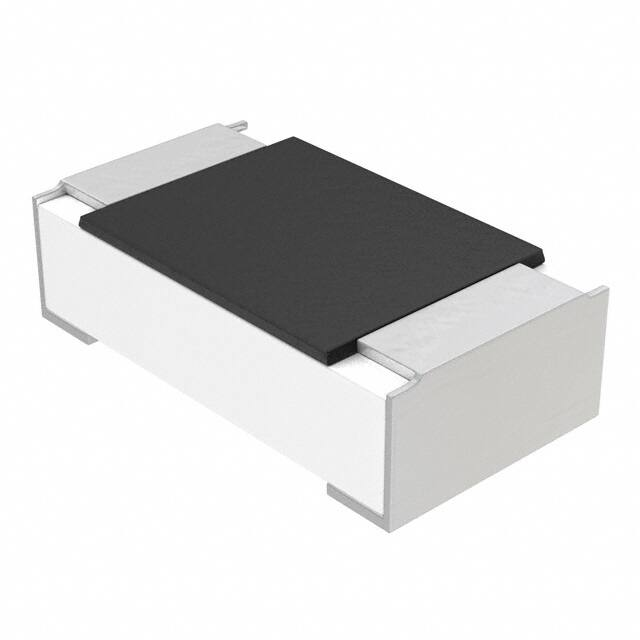
MCS 0402 VG01, MCT 0603 VG01, MCU 0805 VG01, MCA 1206 VG01
www.vishay.com
Vishay Beyschlag
Thin Film Chip Resistors With Established Reliability
FEATURES
• IECQ-CECC approved to EN 140401-801,
version E
• Established reliability, failure rate level E6
• Advanced thin film technology
• Single Lot Date Code
• Material categorization: for definitions of compliance
please see www.vishay.com/doc?99912
MCS 0402 VG01, MCT 0603 VG01, MCU 0805 VG01, and
MCA 1206 VG01 thin film flat chip resistors with established
reliability are the perfect choice for all high-reliability
applications typically found in military, aircraft and
spacecraft electronics. These versions supplement the
families of professional and precision thin film flat chip
resistors MCS 0402, MCT 0603, MCU 0805, and MCA 1206.
APPLICATIONS
• Military
• Avionics
• Space
TECHNICAL SPECIFICATIONS
DESCRIPTION
Imperial size
Metric size code (EN/CECC style)
Resistance range
MCS 0402 VG01
MCT 0603 VG01
MCU 0805 VG01
MCA 1206 VG01
0402
0603
0805
1206
RR1005M
RR1608M
RR2012M
RR3216M
10 Ω to 1 MΩ; 0 Ω
1 Ω to 1 MΩ; 0 Ω
1 Ω to 1 MΩ; 0 Ω
1 Ω to 1 MΩ; 0 Ω
Resistance tolerance
± 1 %; ± 0.1 %
Temperature coefficient
± 50 ppm/K; ± 15 ppm/K
Rated dissipation, P70
Operating voltage, Umax. ACRMS or DC
0.063 W
0.1 W
0.125 W
0.25 W
50 V
75 V
150 V
200 V
Permissible film temperature, ϑF max.
125 °C
Operating temperature range
-55 °C to 125 °C
Max. resistance change at P70 for
resistance, |ΔR/R| max. after:
10 Ω to 1 MΩ
1 Ω to 1 MΩ
≤ 0.25 %
1000 h
8000 h
≤ 0.5 %
225 000 h
≤ 1.5 %
Permissible voltage against ambient
(insulation):
1 min; Uins
Assessed failure rate level
Quality factor, πQ
Failure rate: FITobserved
75 V
100 V
200 V
300 V
E6 = 10-6/h
0.3
< 0.1 x 10⁻⁹/h
Notes
• The failure rate level E6 (10-6/h, πQ = 0.3), corresponding to MIL Level P, is superior to level E5 (10-5/h, πQ = 1) and thus may be used as a
replacement
• These resistors do not feature a limited lifetime when operated within the permissible limits. However, resistance value drift increasing over
operating time may result in exceeding a limit acceptable to the specific application, thereby establishing a functional lifetime
Revision: 16-Jun-2021
Document Number: 28744
1
For technical questions, contact: specialresistors@vishay.com
THIS DOCUMENT IS SUBJECT TO CHANGE WITHOUT NOTICE. THE PRODUCTS DESCRIBED HEREIN AND THIS DOCUMENT
ARE SUBJECT TO SPECIFIC DISCLAIMERS, SET FORTH AT www.vishay.com/doc?91000
�MCS 0402 VG01, MCT 0603 VG01, MCU 0805 VG01, MCA 1206 VG01
www.vishay.com
Vishay Beyschlag
TEMPERATURE COEFFICIENT AND RESISTANCE RANGE
TYPE / SIZE
MCS 0402 VG01
MCT 0603 VG01
MCU 0805 VG01
TCR
TOLERANCE
RESISTANCE
E-SERIES
± 50 ppm/K
±1%
10 Ω to 1 MΩ
E96
± 15 ppm/K
± 0.1 %
100 Ω to 33.2 kΩ
E192
Jumper (1); Imax. = 0.63 A
≤ 20 mΩ
0Ω
-
± 50 ppm/K
±1%
1 Ω to 1 MΩ
E96
± 15 ppm/K
± 0.1 %
100 Ω to 47.5 kΩ
E192
Jumper (1); Imax. = 1 A
≤ 20 mΩ
0Ω
-
± 50 ppm/K
±1%
1 Ω to 1 MΩ
E96
± 15 ppm/K
± 0.1 %
100 Ω to 100 kΩ
E192
≤ 20 mΩ
0Ω
-
± 50 ppm/K
±1%
1 Ω to 1 MΩ
E96
± 15 ppm/K
± 0.1 %
43.2 Ω to 332 kΩ
E192
Jumper (1); Imax. = 2 A
≤ 20 mΩ
0Ω
-
Jumper
MCA 1206 VG01
(1);
Imax. = 1.5 A
Notes
• Other TCR or tolerances, or combinations thereof, or resistance values from other E-series than given are not permitted in EN 140401-801
for version E products
(1) The temperature coefficient of resistance (TCR) is not specified for 0 Ω jumpers
PACKAGING
TYPE / SIZE
CODE
QUANTITY
E1
1000
E0
10 000
P1
1000
P5
5000
P1
1000
P5
5000
P1
1000
P5
5000
PACKAGING
STYLE
MCS 0402 VG01
WIDTH
PITCH
8 mm
2 mm
PACKAGING
DIMENSIONS
MCT 0603 VG01
MCU 0805 VG01
Paper tape
acc. IEC 60286-3,
Type 1a, on reel
Ø 180 mm/7"
8 mm
4 mm
MCA 1206 VG01
Revision: 16-Jun-2021
Document Number: 28744
2
For technical questions, contact: specialresistors@vishay.com
THIS DOCUMENT IS SUBJECT TO CHANGE WITHOUT NOTICE. THE PRODUCTS DESCRIBED HEREIN AND THIS DOCUMENT
ARE SUBJECT TO SPECIFIC DISCLAIMERS, SET FORTH AT www.vishay.com/doc?91000
�MCS 0402 VG01, MCT 0603 VG01, MCU 0805 VG01, MCA 1206 VG01
www.vishay.com
Vishay Beyschlag
PART NUMBER AND PRODUCT DESCRIPTION
Part Number: MCT0603HC2873FP500
Part Number: MCT0603HZ0000ZP500
M
C
T
0
6
0
3
H
C
2
8
7
3
F
P
5
0
0
M
C
T
0
6
0
3
H
Z
0
0
0
0
Z
P
5
0
0
TYPE / SIZE
VERSION
TCR
RESISTANCE
TOLERANCE
PACKAGING
MCS 0402
MCT 0603
MCU 0805
MCA 1206
H = EN 140401-801,
“Version E”;
failure rate level E6
C = ± 50 ppm/K
E = ± 15 ppm/K
Z = jumper
3 digit value
1 digit multiplier
F=±1%
B = ± 0.1 %
Z = jumper
E1
E0
P1
P5
MULTIPLIER
8 = *10-2
9 = *10-1
0 = *100
1 = *101
2 = *102
3 = *103
4 = *104
0000 = jumper
Product Description: MCT 0603-50 1 % VG01 P5 287K
Product Description: MCT 0603 VG01 P5 0R0
MCT 0603
-50
1%
VG01
P5
287K
MCT 0603
-
-
VG01
P5
0R0
TYPE / SIZE
TCR
TOLERANCE
VERSION
PACKAGING
RESISTANCE
MCS 0402
MCT 0603
MCU 0805
MCA 1206
± 50 ppm/K
± 15 ppm/K
±1%
± 0.1 %
VG01 = EN 140401-801,
“Version E”;
failure rate level E6
E1
E0
P1
P5
49R9 = 49.9 Ω
287K = 287 kΩ
0R0 = jumper
Notes
• The products can be ordered using either the PART NUMBER or the PRODUCT DESCRIPTION
• Products within a packaging unit are Single Lot Date Code
EN 140401-801 ORDERING INFORMATION
Example of the ordering information for a resistor: MCT 0603-50 1 % VG01 287K
EN140401-801EZRR1608MR287KFE6
Example of the ordering information for a zero ohm jumper: MCT 0603 VG01 0R0
EN140401-801EZRR1608M-0R00-E6
The elements used in the component number have the following meaning:
EN140401-801
EZ
RR1608M
R
287K
F
E6
EN detail specification number
Assessment level for the zero-defect approach
Style (size)
Temperature coefficient, according to EN 60062
R = ± 50 ppm/K; P = ± 15 ppm/K
Resistance, according to EN 60062, 4 characters
Tolerance on rated resistance, according to EN 60062
F = ± 1 %; B = ± 0.1 %
Failure rate level according to EN 60115-1, annex ZR
Note
• The ordering information according to EN 140401-801:2014 shown above succeeds and replaces the ordering information according to
earlier versions of the detail specification EN 140401-801 or its predecessor CECC 40401-801, for example:
CECC 40401-801 EZ RR1608M C 287K F E6
CECC 40401-801 S RR1608M C 287K F E6
with
EZ; S
Assessment level, where EZ is successor to and superior replacement for S
RR1608M
Style, with suffix M for “metric”
C
Temperature coefficient, according to the detail specification
C = ± 50 ppm/K; E = ± 15 ppm/K
Revision: 16-Jun-2021
Document Number: 28744
3
For technical questions, contact: specialresistors@vishay.com
THIS DOCUMENT IS SUBJECT TO CHANGE WITHOUT NOTICE. THE PRODUCTS DESCRIBED HEREIN AND THIS DOCUMENT
ARE SUBJECT TO SPECIFIC DISCLAIMERS, SET FORTH AT www.vishay.com/doc?91000
�MCS 0402 VG01, MCT 0603 VG01, MCU 0805 VG01, MCA 1206 VG01
www.vishay.com
Vishay Beyschlag
DESCRIPTION
MATERIALS
Production is strictly controlled and follows an extensive
set of instructions established for reproducibility. A
homogeneous film of metal alloy is deposited on a high
grade ceramic substrate (Al2O3) and conditioned to achieve
the desired temperature coefficient. Specially designed
inner contacts are deposited on both sides. A special laser
is used to achieve the target value by smoothly cutting a
meander groove in the resistive layer without damaging the
ceramics. The resistor elements are covered by a protective
coating designed for electrical, mechanical and climatic
protection. The terminations receive a final pure matte tin on
nickel plating.
Vishay acknowledges the following systems for the
regulation of hazardous substances.
• IEC 62474, Material Declaration for Products of and for the
Electrotechnical Industry, with the list of declarable
substances given therein (2)
• The Global Automotive Declarable Substance List
(GADSL) (3)
• The REACH regulation (1907/2006/EC) and the related list
of substances with very high concern (SVHC) (4) for its
supply chain
The products do not contain any of the banned substances
as per IEC 62474, GADSL, or the SVHC list, see
www.vishay.com/how/leadfree.
Hence the products fully comply with the following
directives:
• 2000/53/EC End-of-Life Vehicle Directive (ELV) and
Annex II (ELV II)
• 2011/65/EU Restriction of the Use of Hazardous
Substances
Directive
(RoHS)
with
amendment
2015/863/EU
• 2012/19/EU Waste Electrical and Electronic Equipment
Directive (WEEE)
Vishay pursues the elimination of conflict minerals from its
supply chain, see the Conflict Minerals Policy at
www.vishay.com/doc?49037.
The result of the determined production is verified by an
extensive testing procedure performed on 100 % of the
individual resistors. This includes pulse load screening for
the elimination of products with a potential risk of early life
failures according to EN 140401-801, 2.1.2.2 (feasible for
R ≥ 10 Ω). Only accepted products are laid directly into the
paper tape in accordance with IEC 60 286-3 (1), Type 1a.
Products within a packaging unit are from the same
production lot and carry the same date code.
ASSEMBLY
The resistors are suitable for processing on automatic SMD
assembly systems. They are suitable for automatic
soldering using wave, reflow or vapor phase as shown in
IEC 61760-1 (1). Solderability is specified for 2 years after
production or requalification. The permitted storage time is
20 years.
The resistors are RoHS-compliant; the pure matte tin plating
provides compatibility with lead (Pb)-free soldering
processes. The immunity of the plating against tin whisker
growth has been proven under extensive testing.
The encapsulation is resistant to all cleaning solvents
commonly used in the electronics industry, including
alcohols, esters and aqueous solutions. The suitability of
conformal coatings, potting compounds, and their
processes, if applied, shall be qualified by appropriate
means to ensure the long-term stability of the whole system.
APPROVALS
The resistors are approved within the IECQ-CECC Quality
Assessment System for Electronic Components to the detail
specification EN 140 401-801 which refers to EN 60115-1,
EN 60115-8, and the variety of environmental test
procedures of the IEC 60068 (1) series.
Conformity is attested by the use of the CECC logo (
) as
the mark of conformity on the package label.
Vishay
Beyschlag
has
achieved
“Approval
of
Manufacturer” in accordance with IECQ 03-1. The release
certificate for “Technology Approval Schedule” in
accordance with CECC 240001 and based on IECQ 03-3-1
is granted for the Vishay Beyschlag manufacturing process.
The Vishay Beyschlag production facility is registered with
the CAGE code D9539.
RELATED PRODUCTS
A wider range of TCR, tolerance and resistance values, plus
the option of values from a different E series is available with
products approved to EN 140401-801, Version A, without
established reliability, nominal failure rate level E0 (quality
factor πQ = 3). See the datasheets:
• “Professional Thin Film Chip Resistors”
(www.vishay.com/doc?28705)
• “Precision Thin Film Chip Resistors”
(www.vishay.com/doc?28700)
Notes
(1) The quoted IEC standards are also released as EN standards with the same number and identical contents
(2) The IEC 62474 list of declarable substances is maintained in a dedicated database, which is available at http://std.iec.ch/iec62474
(3) The Global Automotive Declarable Substance List (GADSL) is maintained by the American Chemistry Council, and available at
www.gadsl.org
(4) The SVHC list is maintained by the European Chemical Agency (ECHA) and available at http://echa.europa.eu/candidate-list-table
Revision: 16-Jun-2021
Document Number: 28744
4
For technical questions, contact: specialresistors@vishay.com
THIS DOCUMENT IS SUBJECT TO CHANGE WITHOUT NOTICE. THE PRODUCTS DESCRIBED HEREIN AND THIS DOCUMENT
ARE SUBJECT TO SPECIFIC DISCLAIMERS, SET FORTH AT www.vishay.com/doc?91000
�MCS 0402 VG01, MCT 0603 VG01, MCU 0805 VG01, MCA 1206 VG01
www.vishay.com
Vishay Beyschlag
Power Dissipation P
FUNCTIONAL PERFORMANCE
0.3
MCA 1206 VG01
MCU 0805 VG01
MCT 0603 VG01
MCS 0402 VG01
W
0.2
0.1
0
-50
0
50
70
100
125 °C 150
Ambient Temperature ϑamb
Current Noise Voltage Ratio
Derating
MCA 1206 VG01
MCU 0805 VG01
MCT 0603 VG01
MCS 0402 VG01
1
µV/V
0.1
0.01
100
1K
10K
:
100K
1M
Resistance Value R
In accordance with IEC 60195
Third Harmonic Ratio A3
Current Noise Voltage Ratio
120
dB
100
80
60
MCA 1206 VG01
MCU 0805 VG01
MCT 0603 VG01
MCS 0402 VG01
40
10
100
1K
In accordance with IEC 60440
10K
100K
:
1M
Resistance Value R
Non-Linearity - Third Harmonic Ratio A3
Further information on the performance of these products is given in the following datasheets:
• “Professional Thin Film Chip Resistors” (www.vishay.com/doc?28705) for products ± 50 ppm/K; ± 1 % and 0 Ω jumper
• “Precision Thin Film Chip Resistors” (www.vishay.com/doc?28700) for products ± 15 ppm/K; ± 0.1 %
Revision: 16-Jun-2021
Document Number: 28744
5
For technical questions, contact: specialresistors@vishay.com
THIS DOCUMENT IS SUBJECT TO CHANGE WITHOUT NOTICE. THE PRODUCTS DESCRIBED HEREIN AND THIS DOCUMENT
ARE SUBJECT TO SPECIFIC DISCLAIMERS, SET FORTH AT www.vishay.com/doc?91000
�MCS 0402 VG01, MCT 0603 VG01, MCU 0805 VG01, MCA 1206 VG01
www.vishay.com
Vishay Beyschlag
TESTS AND REQUIREMENTS
All tests are carried out in accordance with the following specifications:
EN 60115-1, generic specification
EN 60115-8 (successor of EN 140400), sectional specification
EN 140401-801, detail specification
For further information on the tests and requirements of these products please refer to the specifications mentioned above, and
to the following datasheets:
• “Professional Thin Film Chip Resistors” (www.vishay.com/doc?28705) for products ± 50 ppm/K; ± 1 % and 0 Ω jumper
• “Precision Thin Film Chip Resistors” (www.vishay.com/doc?28700) for products ± 15 ppm/K; ± 0.1 %
DIMENSIONS
L
Tt
WT
W
H
Tb
DIMENSIONS AND MASS
H
(mm)
TYPE / SIZE
L
(mm)
W
(mm)
WT
(mm)
MCS 0402 VG01
0.32 ± 0.05
1.0 ± 0.05
0.5 ± 0.05
MCT 0603 VG01
0.45 + 0.1/- 0.05
1.55 ± 0.05
0.85 ± 0.1
MCU 0805 VG01
0.45 + 0.1/- 0.05
2.0 ± 0.1
1.25 ± 0.15
MCA 1206 VG01
0.55 ± 0.1
3.2 + 0.1/- 0.2
1.6 ± 0.15
Tt
(mm)
Tb
(mm)
MASS
(mg)
0.2 + 0.1/- 0.15
0.2 ± 0.1
0.6
> 75 % of W
0.3 + 0.15/- 0.2
1.9
0.4 + 0.1/- 0.2
4.6
0.5 ± 0.25
9.2
Note
• Resistors MCA 1206 VG01 and MCU 0805 VG01 are marked according to the four-character code system of IEC 60062 (1), 4.2.3.
Resistors MCT 0603 VG01 and MCS 0402 VG01 do not show any marking on their blue protective coating
SOLDER PAD DIMENSIONS
X
G
Y
Z
RECOMMENDED SOLDER PAD DIMENSIONS
WAVE SOLDERING
TYPE / SIZE
G
(mm)
Y
(mm)
X
(mm)
REFLOW SOLDERING
Z
(mm)
G
(mm)
Y
(mm)
X
(mm)
Z
(mm)
MCS 0402 VG01
-
-
-
-
0.35
0.55
0.55
1.45
MCT 0603 VG01
0.55
1.10
1.10
2.75
0.65
0.70
0.95
2.05
MCU 0805 VG01
0.80
1.25
1.50
3.30
0.90
0.90
1.40
2.70
MCA 1206 VG01
1.40
1.50
1.90
4.40
1.50
1.15
1.75
3.80
Notes
• The given solder pad dimensions reflect the considerations for board design and assembly as outlined e.g. in standards IEC 61188-5-x (1),
or in publication IPC 7351. They do not guarantee any supposed thermal properties, however, they will be found adequate for most general
applications
(1)
The quoted IEC standards are also released as EN standards with the same number and identical contents
Revision: 16-Jun-2021
Document Number: 28744
6
For technical questions, contact: specialresistors@vishay.com
THIS DOCUMENT IS SUBJECT TO CHANGE WITHOUT NOTICE. THE PRODUCTS DESCRIBED HEREIN AND THIS DOCUMENT
ARE SUBJECT TO SPECIFIC DISCLAIMERS, SET FORTH AT www.vishay.com/doc?91000
�MCS 0402 VG01, MCT 0603 VG01, MCU 0805 VG01, MCA 1206 VG01
www.vishay.com
Vishay Beyschlag
HISTORICAL 12NC INFORMATION
• The resistors had a 12-digit code starting with 2312
RESISTANCE DECADE
LAST DIGIT
1 Ω to 9.99 Ω
8
• The subsequent 4 digits indicated the resistor type,
specification and packaging; see the 12NC table
• The remaining 4 digits indicate the resistance value:
-The first 3 digits indicated the resistance value
- The last digit indicated the resistance decade in
accordance with the resistance decade table
10 Ω to 99.9 Ω
9
100 Ω to 999 Ω
1
1 kΩ to 9.99 kΩ
2
10 kΩ to 99.9 kΩ
3
100 kΩ to 999 kΩ
4
1 MΩ
5
Historical 12NC Example
The 12NC of a MCT 0603 VG01 resistor, value 287K and
TCR 50 with ± 1 % tolerance, supplied in cardboard tape of
5000 units per reel was: 2312 215 02874.
HISTORICAL 12NC - Resistor type and packaging
2312 ... .....
DESCRIPTION
TOL.
E1
1000 PIECES
± 50 ppm/K
±1%
260 0....
275 0....
± 15 ppm/K
± 0.1 %
262 0....
277 0....
TYPE
MCS 0402 VG01
CARDBOARD TAPE ON REEL
TCR
Jumper
262 90001
TOL.
P5
5000 PIECES
PW
20 000 PIECES
± 50 ppm/K
±1%
200 0....
215 0....
205 0....
± 15 ppm/K
± 0.1 %
202 0....
217 0....
-
202 90001
217 90001
207 90001
245 0....
TCR
Jumper
MCU 0805 VG01
± 50 ppm/K
±1%
240 0....
255 0....
± 15 ppm/K
± 0.1 %
242 0....
257 0....
-
242 90001
257 90001
247 90001
Jumper
MCA 1206 VG01
277 90001
P1
1000 PIECES
TYPE
MCT 0603 VG01
E0
10 000 PIECES
± 50 ppm/K
±1%
± 15 ppm/K
± 0.1 %
No 12NC assigned to MCA 1206 VG01
Jumper
Revision: 16-Jun-2021
Document Number: 28744
7
For technical questions, contact: specialresistors@vishay.com
THIS DOCUMENT IS SUBJECT TO CHANGE WITHOUT NOTICE. THE PRODUCTS DESCRIBED HEREIN AND THIS DOCUMENT
ARE SUBJECT TO SPECIFIC DISCLAIMERS, SET FORTH AT www.vishay.com/doc?91000
�Legal Disclaimer Notice
www.vishay.com
Vishay
Disclaimer
ALL PRODUCT, PRODUCT SPECIFICATIONS AND DATA ARE SUBJECT TO CHANGE WITHOUT NOTICE TO IMPROVE
RELIABILITY, FUNCTION OR DESIGN OR OTHERWISE.
Vishay Intertechnology, Inc., its affiliates, agents, and employees, and all persons acting on its or their behalf (collectively,
“Vishay”), disclaim any and all liability for any errors, inaccuracies or incompleteness contained in any datasheet or in any other
disclosure relating to any product.
Vishay makes no warranty, representation or guarantee regarding the suitability of the products for any particular purpose or
the continuing production of any product. To the maximum extent permitted by applicable law, Vishay disclaims (i) any and all
liability arising out of the application or use of any product, (ii) any and all liability, including without limitation special,
consequential or incidental damages, and (iii) any and all implied warranties, including warranties of fitness for particular
purpose, non-infringement and merchantability.
Statements regarding the suitability of products for certain types of applications are based on Vishay's knowledge of typical
requirements that are often placed on Vishay products in generic applications. Such statements are not binding statements
about the suitability of products for a particular application. It is the customer's responsibility to validate that a particular product
with the properties described in the product specification is suitable for use in a particular application. Parameters provided in
datasheets and / or specifications may vary in different applications and performance may vary over time. All operating
parameters, including typical parameters, must be validated for each customer application by the customer's technical experts.
Product specifications do not expand or otherwise modify Vishay's terms and conditions of purchase, including but not limited
to the warranty expressed therein.
Hyperlinks included in this datasheet may direct users to third-party websites. These links are provided as a convenience and
for informational purposes only. Inclusion of these hyperlinks does not constitute an endorsement or an approval by Vishay of
any of the products, services or opinions of the corporation, organization or individual associated with the third-party website.
Vishay disclaims any and all liability and bears no responsibility for the accuracy, legality or content of the third-party website
or for that of subsequent links.
Except as expressly indicated in writing, Vishay products are not designed for use in medical, life-saving, or life-sustaining
applications or for any other application in which the failure of the Vishay product could result in personal injury or death.
Customers using or selling Vishay products not expressly indicated for use in such applications do so at their own risk. Please
contact authorized Vishay personnel to obtain written terms and conditions regarding products designed for such applications.
No license, express or implied, by estoppel or otherwise, to any intellectual property rights is granted by this document or by
any conduct of Vishay. Product names and markings noted herein may be trademarks of their respective owners.
© 2021 VISHAY INTERTECHNOLOGY, INC. ALL RIGHTS RESERVED
Revision: 09-Jul-2021
1
Document Number: 91000
�


 工商网监
湘ICP备2023018690号
工商网监
湘ICP备2023018690号
