OLED-128O064D-LPP3N00000
www.vishay.com
Vishay
128 x 64 Graphic OLED
FEATURES
• Type: graphic
• Display format: 128 x 64 dots
• Built-in controller: SSD1306
• Duty cycle: 1/64
• +3 V power supply
• Interface: 6800, 8080, serial, and I2C
• Material categorization: for definitions of compliance
please see www.vishay.com/doc?99912
MECHANICAL DATA
ITEM
ABSOLUTE MAXIMUM RATINGS
STANDARD VALUE
Module dimension
UNIT
ITEM
26.7 x 19.26 x 1.65
Viewing area
23.938 x 12.058
Active area
21.738 x 10.858
Dot size
0.148 x 0.148
Dot pitch
0.17 x 0.17
Mounting hole
mm
n/a
SYMBOL
STANDARD VALUE
MIN.
MAX.
Supply voltage
for logic (1)(2)
VDD
0
3.3
Supply voltage
for display (1)(2)
VCC
0
15
Operating temperature
TOP
-40
+80
Storage temperature
TSTG
-40
+80
UNIT
V
°C
Notes
(1) All the above voltages are on the basis of “V
SS = 0 V”.
(2) When this module is used beyond the above absolute maximum
ratings, permanent breakage of the module may occur. Also, for
normal operations, it is desirable to use this module under the
conditions according to section 6 “Electrical Characteristics”. If
this module is used beyond these conditions, malfunctioning of
the module can occur and the reliability of the module may
deteriorate.
ELECTRICAL CHARACTERISTICS
ITEM
SYMBOL
CONDITION
Supply voltage for logic
VDD
Supply voltage for display
VCC
Input high voltage
STANDARD VALUE
UNIT
MIN.
TYP.
MAX.
-
2.4
2.8
3.3
-
10
12
15
VIH
-
0.8 VDD
-
VDDI/O
Input low voltage
VIL
-
0
-
0.2 VDD
Output high voltage
VOH
-
0.9 VDD
-
VDDI/O
Output low voltage
VOL
-
0
-
0.1 VDD
50 % check board operating current
ICC
VCC = 12 V
4.0
6.0
7.5
V
mA
OPTIONS
EMITTING COLOR
YELLOW
GREEN
RED
BLUE
WHITE
Yes
-
-
-
-
Document Number: 37904
1
For technical questions, contact: displays@vishay.com
THIS DOCUMENT IS SUBJECT TO CHANGE WITHOUT NOTICE. THE PRODUCTS DESCRIBED HEREIN AND THIS DOCUMENT
ARE SUBJECT TO SPECIFIC DISCLAIMERS, SET FORTH AT www.vishay.com/doc?91000
Revision: 14-Dec-16
�OLED-128O064D-LPP3N00000
www.vishay.com
Vishay
INTERFACE PIN FUNCTION
PIN NO.
SYMBOL
FUNCTION
1
NC (GND)
Reserved pin (supporting pin)
The supporting pins can reduce the influences from stresses on the function pins. These pins must be connected
to external ground.
2
3
4
5
C2N
C2P
C1P
C1N
Positive terminal of the flying inverting capacitor negative terminal of the flying boost capacitor
The charge-pump capacitors are required between the terminals. They must be floated when the converter is not
used.
6
VBAT
Power supply for DC/DC converter circuit
This is the power supply pin for the internal buffer of the DC/DC voltage converter. It must be connected to external
source when the converter is used. It should be connected to VDD when the converter is not used.
7
NC
NC
8
VSS
Ground of logic circuit
This is a ground pin. It also acts as a reference for the logic pins. It must be connected to external ground.
9
VDD
Power supply for logic
This is a voltage supply pin. It must be connected to external source.
10
BS0
Communicating protocol select
These pins are MCU interface selection input. See the following table:
11
BS1
12
BS2
13
CS#
Chip select
This pin is the chip select input. The chip is enabled for MCU communication only when CS# is pulled low.
14
RES#
Power reset for controller and driver
This pin is reset signal input. When the pin is low, initialization of the chip is executed.
D / C#
Data / command control
This pin is data / command control pin. When the pin is pulled high, the input at D7 to D0 is treated as display data.
When the pin is pulled low, the input at D7 to D0 will be transferred to the command register. For detail relationship
to MCU interface signals, please refer to the timing characteristics diagrams. When the pin is pulled high and serial
interface mode is selected, the data at SDIN is treated as data. When it is pulled low, the data at SDIN will be
transferred to the command register. In I2C mode, this pin acts as SA0 for slave address selection.
R / W#
Read / write select or write
This pin is MCU interface input. When interfacing to a 68XX-series microprocessor, this pin will be used as read /
write (R / W#) selection input. Pull this pin to “high” for read mode and pull it to “low” for write mode.
When 80XX interface mode is selected, this pin will be the write (WR#) input. Data write operation is initiated when
this pin is pulled low and the CS# is pulled low.
E / RD#
Read / write enable or read
This pin is MCU interface input. When interfacing to a 68XX-series microprocessor, this pin will be used as the
enable (E) signal. Read / write operation is initiated when this pin is pulled high and the CS# is pulled low.
When connecting to an 80XX-microprocessor, this pin receives the read (RD#) signal. Data read operation is
initiated when this pin is pulled low and CS# is pulled low.
D0 to D7
Host data input / output bus
These pins are 8-bit bi-directional data bus to be connected to the microprocessor’s data bus. When serial mode
is selected, D1 will be the serial data input SDIN and D0 will be the serial clock input SCLK. When I2C mode is
selected, D2 and D1 should be tired together and serve as SDAout and SDAin in application and D0 is the serial
clock input SCL.
26
IREF
Current reference for brightness adjustment
This pin is segment current reference pin. A resistor should be connected between this pin and VSS. Set the current
lower than 12.5 μA.
27
VCOMH
Voltage output high level for COM signal
This pin is the input pin for the voltage output high level for COM signals. A capacitor should be connected between
this pin and VSS.
28
VCC
Power supply for OEL panel
This is the most positive voltage supply pin of the chip. A stabilization capacitor should be connected between this
pin and VSS when the converter is used. It must be connected to external source when the converter is not used.
29
VLSS
Ground of analog circuit
This is an analog ground pin. It should be connected to VSS externally.
30
NC (GND)
15
16
17
18 to 25
BS0
BS1
BS2
I2C
0
1
0
3-wire SPI
1
0
0
4-wire SPI
0
0
0
8-bit 68XX parallel
0
0
1
8-bit 80XX parallel
0
1
1
Reserved pin (supporting pin)
The supporting pins can reduce the influences from stresses on the function pins. These pins must be connected
to external ground.
Document Number: 37904
2
For technical questions, contact: displays@vishay.com
THIS DOCUMENT IS SUBJECT TO CHANGE WITHOUT NOTICE. THE PRODUCTS DESCRIBED HEREIN AND THIS DOCUMENT
ARE SUBJECT TO SPECIFIC DISCLAIMERS, SET FORTH AT www.vishay.com/doc?91000
Revision: 14-Dec-16
�OLED-128O064D-LPP3N00000
www.vishay.com
Vishay
26.7 ± 0.2
25.7 (polarizer)
23.938 (VA)
21.738 (AA)
0.5
1.381
2.481
10.0
1.65 ± 0.3
0.7
0.7
5.0
8.0
(31.26)
19.26 ± 0.2
15.5 ± 0.2
14.4 (polarizer)
12.058 (VA)
10.858 (AA)
0.5
1.841
2.441
DIMENSIONS in millimeters
Active area 0.96"
128 x 64 pixels
Remove tape
Polarizer
Glue
2 x R0.8 ± 0.05
12.0
16 (alignment mark)
P0.70 x (30 - 1) = 20.3 (W0.40 ± 0.03)
0.85 ± 0.1
22.0
0.148
(2.35)
0.1
Contact side
30
1
0.17
Contact side
12.0
11.0
6.887
4.75
4.0
2.0
Shading tape
0.17
0.148
Segment 127
(column 1)
SCALE: 20/1
Segment 0
(column 128)
Common 32
(row 63)
Common 0
(row 64)
Common 63
(row 1)
Common 31
(row 2)
The non-specified tolerance of dimension is ± 0.3 mm.
Document Number: 37904
3
For technical questions, contact: displays@vishay.com
THIS DOCUMENT IS SUBJECT TO CHANGE WITHOUT NOTICE. THE PRODUCTS DESCRIBED HEREIN AND THIS DOCUMENT
ARE SUBJECT TO SPECIFIC DISCLAIMERS, SET FORTH AT www.vishay.com/doc?91000
Revision: 14-Dec-16
�OLED-128O064D-LPP3N00000
www.vishay.com
Vishay
1. Module Classification Information
OLED
128
O
064 D
L P P 3
N 00000
� ���������ۑ
� ������ۑ
� �����ۑ
� ������ۑ
� ����ۑ
� ���ۑ
� ����ۑ
� ����չ����պ�������ջ� �
ġġġ ۑ
�
1
Brand烉Vishay Intertechnology, Inc.
2
Horizontal Format烉 128 characters
3
Display Type烉Nĺ&KDUDFWHU�7\SH��Hĺ*UDSKLF�7\SH� � ��
很抱歉,暂时无法提供与“O128O064DLPP3N0000”相匹配的价格&库存,您可以联系我们找货
免费人工找货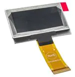


 工商网监
湘ICP备2023018690号
工商网监
湘ICP备2023018690号
