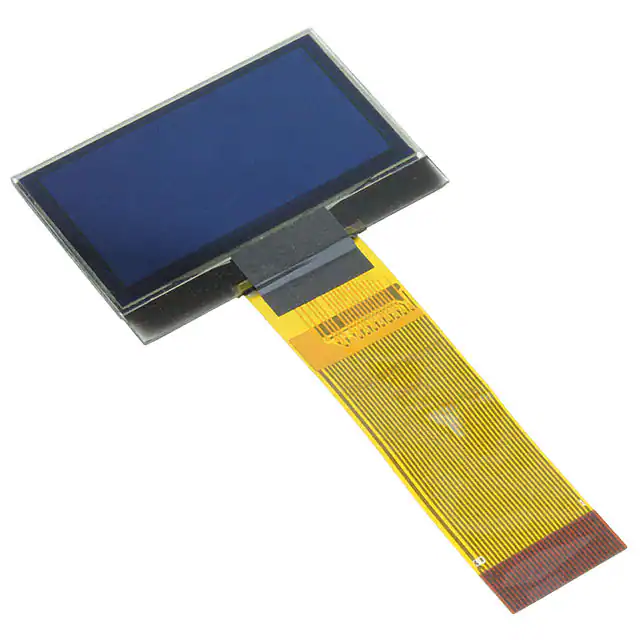
OLED-128O064F-LPP3N00000
www.vishay.com
Vishay
128 x 64 Graphic OLED
FEATURES
• Type: graphic
• Display format: 128 x 64 dots
• Built-in controller: SSD1325
• Duty cycle: 1/64
• +3 V power supply
• Interface: 6800, 8080, SPI, I2C
• With polarizer
• Material categorization: for definitions of compliance
please see www.vishay.com/doc?99912
MECHANICAL DATA
ITEM
ABSOLUTE MAXIMUM RATINGS
STANDARD VALUE
Module dimension
UNIT
ITEM
41.8 x 27.9 x 1.8
Viewing area
38.45 x 20.21
Active area
36.45 x 18.21
Dot size
0.255 x 0.255
Dot pitch
0.285 x 0.285
Mounting hole
mm
n/a
SYMBOL
STANDARD VALUE
MIN.
MAX.
Supply voltage
for logic (1)(2)
VDD
-0.3
4
Supply voltage
for display (1)(2)
VCC
0
15
Operating
temperature
TOP
-40
+80
Storage
temperature
TSTG
-40
+80
UNIT
V
°C
Notes
(1) All the above voltages are on the basis of “V
SS = 0 V”
(2) When this module is used beyond the above absolute maximum
ratings, permanent breakage of the module may occur. Also,
for normal operations, it is desirable to use this module under
the conditions according to “Electrical Characteristics”. If this
module is used beyond these conditions, malfunctioning of the
module can occur and the reliability of the module may
deteriorate
ELECTRICAL CHARACTERISTICS
ITEM
SYMBOL
CONDITION
Supply voltage for logic
VDD
Supply voltage for display
VCC
Input high voltage
Input low voltage
STANDARD VALUE
MIN.
TYP.
MAX.
-
2.8
3.0
3.3
-
13.5
14
14.5
VIH
-
0.8 VDD
-
VDD
VIL
-
0
-
0.2 VDD
Output high voltage
VOH
-
0.9 VDD
-
VDD
Output low voltage
VOL
-
0
-
0.1 VDD
50 % check board operating current
ICC
VCC = 14 V
12
13
15
UNIT
V
mA
OPTIONS
EMITTING COLOR
YELLOW
GREEN
RED
BLUE
WHITE
Yes
-
-
-
-
Document Number: 37907
1
For technical questions, contact: displays@vishay.com
THIS DOCUMENT IS SUBJECT TO CHANGE WITHOUT NOTICE. THE PRODUCTS DESCRIBED HEREIN AND THIS DOCUMENT
ARE SUBJECT TO SPECIFIC DISCLAIMERS, SET FORTH AT www.vishay.com/doc?91000
Revision: 17-Aug-17
�OLED-128O064F-LPP3N00000
www.vishay.com
Vishay
INTERFACE PIN FUNCTION
PIN NO.
SYMBOL
1
NC (GND)
FUNCTION
2
VCC
3
VCOMH
This pin is the input pin for the voltage output high level for COM signals. It can be supplied externally or
internally. When VCOMH is generated internally, a capacitor should be connected between this pin and VSS
4
IREF
This pin is segment current reference pin. A resistor should be connected between this pin and VSS. Set the
current at 10 μA
D0 to D7
These pins are 8-bit bi-directional data bus to be connected to the microprocessor’s data bus. When serial
mode is selected, D1 will be the serial data input SDIN and D0 will be the serial clock input SCLK
13
E / RD#
This pin is MCU interface input. When interfacing to a 6800-series microprocessor, this pin will be used as
the enable (E) signal. Read / write operation is initiated when this pin is pulled “high” and the CS# is pulled
“low”. When connecting to an 8080-microprocessor, this pin receives the read (RD#) signal. Data read
operation is initiated when this pin is pulled “low” and CS# is pulled “low”
14
R / W#
This pin is MCU interface input. When interfacing to a 6800-series microprocessor, this pin will be used as
read / write (R / W#) selection input. Pull this pin to “high” for read mode and pull it to “low” for write mode.
When 8080 interface mode is selected, this pin will be the write (WR#) input. Data write operation is initiated
when this pin is pulled “low” and the CS# is pulled “low”
15
D / C#
This pin is data / command control pin. When the pin is pulled “high”, the input at D7 to D0 is treated as
display data. When the pin is pulled low, the input at D7 to D0 will be transferred to the command register.
For detail relationship to MCU interface signals, please refer to the timing characteristics diagrams
16
RES#
This pin is reset signal input. When the pin is “low”, initialization of the chip is executed
17
CS#
This pin is the chip select input. The chip is enabled for MCU communication only when CS# is pulled “low”
18
NC
No connection
Power supply for OLED panel
This is the most positive voltage supply pin of the chip. It must be supplied externally
5
6
7
8
9
10
11
12
No connection
Communicating protocol select. These pins are MCU interface selection input. See the following table:
19
BS2
20
BS1
21
NC
No connection
22
NC
No connection
23
NC
No connection
24
NC
No connection
25
NC
No connection
26
NC
No connection
27
NC
No connection
28
NC
No connection
29
VSS
This is a ground pin. It also acts as a reference for the logic pins and the OLED driving voltages. It must be
connected to external ground
30
VSL
This pin is the output pin for the voltage output low level for SEG signals. A capacitor should be connected
between this pin and VSS
68XX-parallel
80XX-parallel
Serial
I2C
BS1
0
1
0
1
BS2
1
1
0
0
Document Number: 37907
2
For technical questions, contact: displays@vishay.com
THIS DOCUMENT IS SUBJECT TO CHANGE WITHOUT NOTICE. THE PRODUCTS DESCRIBED HEREIN AND THIS DOCUMENT
ARE SUBJECT TO SPECIFIC DISCLAIMERS, SET FORTH AT www.vishay.com/doc?91000
Revision: 17-Aug-17
�OLED-128O064F-LPP3N00000
www.vishay.com
Vishay
DIMENSIONS in millimeters
41.8 ± 0.2
40.8 (polarizer)
38.45 (VA)
1.675
0.85
1.85
20.21 (VA)
18.21 (AA)
27.9 ± 0.2
22.14 (polarizer)
1.8 ± 0.2
36.45 (AA)
2.675
Remove tape
t = 0.15 mm max.
Active area 1.6 ''
128 x 64 pixels
Polarizer
t = 0.25 mm
0.7 ± 0.07
0.7 ± 0.07
Shade film
t = 0.1 mm
V COMH
VCC
NC(GND )
D5
D6
D1
D2
D7
D3
D4
IREF
NC
CS#
R /W#
E /RD#
D0
D /C#
RES#
BS2
NC
Vss
NC
VDD
NC
BS1
VSL
NC
NC
NC
30
NC
6.0 ± 0.5
3.0 ± 0.5
50.0 ± 0.5
Protective tape
1
Stiffener
0.35
P0.5 x 29 = 14.5 ± 0.05
13.15 ± 05
Contact side
0.3 ± 0.05
15.5 ± 0.1
Common 62
(row 2)
Common 63
(row 1)
Common 0
(row 64)
Common 1
(row 63)
Segment 127
(column 1)
Segment 0
(column 128)
SCALE 3/2
0.255
0.285
0.285
0.255
Dot sizes
The non-specific tolerance of dimensions is ± 0.3 mm.
Document Number: 37907
3
For technical questions, contact: displays@vishay.com
THIS DOCUMENT IS SUBJECT TO CHANGE WITHOUT NOTICE. THE PRODUCTS DESCRIBED HEREIN AND THIS DOCUMENT
ARE SUBJECT TO SPECIFIC DISCLAIMERS, SET FORTH AT www.vishay.com/doc?91000
Revision: 17-Aug-17
�OLED-128O064F-LPP3N00000
www.vishay.com
Vishay
MODULE CLASSIFICATION INFORMATION
OLED
-
1
128
O
064
F
2
3
4
5
-
L
P
P
3
N
0
0
000
6
7
8
9
10
11
12
13
1
Brand
Vishay Intertechnology, Inc.
2
Horizontal format
128 columns
F: COG type, with frame
H: graphic type
3
Display type
N: character type
O: COG type
Y: tab type
4
Vertical format
5
Serials code
64 lines
F
A: amber
B: blue
C: full color
G: green
6
Emitting color
L: yellow
R: red
S: sky blue
W: white
X: yellow / sky blue (dual color)
Y: yellow green
7
Polarizer
8
Display mode
9
Driver voltage
10
Touch panel
N: without polarizer
P: with polarizer
A: active matrix
P: passive matrix
3: 3.0 V to 3.3 V
5: 5.0 V
N: without touch panel
T: with touch panel
0: standard
1: sunlight readable
11
Products type
2: transparent OLED (TOLED)
3: flexible OLED
4: OLED for lighting
0: standard (A level)
2: B level
12
Product grades
3: C level
4: high class (AA level)
5: customer offerings
13
Serial number
Application serial number (000 to ZZZ)
Document Number: 37907
4
For technical questions, contact: displays@vishay.com
THIS DOCUMENT IS SUBJECT TO CHANGE WITHOUT NOTICE. THE PRODUCTS DESCRIBED HEREIN AND THIS DOCUMENT
ARE SUBJECT TO SPECIFIC DISCLAIMERS, SET FORTH AT www.vishay.com/doc?91000
Revision: 17-Aug-17
�OLED-128O064F-LPP3N00000
www.vishay.com
Vishay
GENERAL SPECIFICATIONS
ITEM
DIMENSION
Number of characters
128 x 64 dots
Module dimension
UNIT
41.8 x 27.9 x 1.8
mm
View area
38.45 x 20.21
mm
Active area
36.45 x 18.21
mm
Dot size
0.255 x 0.255
mm
Dot pitch
0.285 x 0.285
mm
Panel type
OLED, yellow
Duty
1/64
IC
SSD1325
FUNCTION BLOCK DIAGRAM
128 columns
128 x 64
SSD1325
dot matrixes
64 rows
Note
• For more information, please refer to Application Note provided by Vishay
Document Number: 37907
5
For technical questions, contact: displays@vishay.com
THIS DOCUMENT IS SUBJECT TO CHANGE WITHOUT NOTICE. THE PRODUCTS DESCRIBED HEREIN AND THIS DOCUMENT
ARE SUBJECT TO SPECIFIC DISCLAIMERS, SET FORTH AT www.vishay.com/doc?91000
Revision: 17-Aug-17
�OLED-128O064F-LPP3N00000
www.vishay.com
Vishay
OPTICAL CHARACTERISTICS
ITEM
SYMBOL
View angle
Contrast ratio
MIN.
TYP.
MAX.
(V)θ
160
-
-
(H)ϕ
160
-
-
2000 : 1
-
-
-
-
10
-
μs
-
10
-
μs
60
80
-
cd/m2
CR
CONDITION
Dark
trise
Response time
tfall
Display with 50 % check board brightness
CIEx (yellow)
(CIE1931)
0.45
0.47
0.49
CIEy (yellow)
(CIE1931)
0.48
0.50
0.52
UNIT
deg
OLED LIFETIME
ITEM
Operating life time
CONDITIONS
MIN.
TYP.
TA = 25 °C, initial 50 % check board brightness typical value
50 000 h
-
Notes
• Life time is defined the amount of time when the luminance has decayed to < 50 % of the initial value
• This analysis method uses life data obtained under accelerated conditions to extrapolate an estimated probability density function (PDF) for
the product under normal use conditions
• Screen saving mode will extend OLED lifetime
Document Number: 37907
6
For technical questions, contact: displays@vishay.com
THIS DOCUMENT IS SUBJECT TO CHANGE WITHOUT NOTICE. THE PRODUCTS DESCRIBED HEREIN AND THIS DOCUMENT
ARE SUBJECT TO SPECIFIC DISCLAIMERS, SET FORTH AT www.vishay.com/doc?91000
Revision: 17-Aug-17
�OLED-128O064F-LPP3N00000
www.vishay.com
Vishay
RELABILITY
ENVIRONMENTAL TEST
TEST ITEM
High temperature storage
Low temperature storage
High temperature operation
Low temperature operation
High temperature /
humidity storage
CONTENT OF TEST
TEST CONDITION
Endurance test applying the high storage temperature for a
long time
Endurance test applying the low storage temperature for a
long time
Endurance test applying the electric stress (voltage and
current) and the thermal stress to the element for a long time
Endurance test applying the electric stress under low
temperature for a long time
Endurance test applying the high temperature and high
humidity storage for a long time
Endurance test applying the low and high temperature cycle
-40 °C
25 °C
80 °C
Temperature cycle
80 °C, 240 h
-40 °C, 240 h
80 °C, 240 h
-40 °C, 240 h
60 °C, 90 % RH, 240 h
-40 °C / 80 °C, 100 cycles
30 min
5 min
1 cycle
30 min
MECHANICAL TEST
Vibration test
Endurance test applying the vibration during transportation
and using
10 Hz to 22 Hz for 1.5 mm peak-to-peak,
22 Hz to 500 Hz for 1.5 g,
total 0.5 h
Shock test
Constructional and mechanical endurance test applying the
shock during transportation
50 g half sin wave 11 ms,
3 times of each direction
Atmospheric pressure test
Endurance test applying the atmospheric pressure during
transportation by air
115 mbar, 40 h
OTHERS
Static electricity test
Endurance test applying the electric stress to the terminal
VS = ± 600 V (contact), ± 800 V (air),
RS = 330 Ω, CS = 150 pF, 10 times
Note
• Supply voltage for OLED system = operating voltage at 25 °C
TEST AND MEASUREMENT CONDITIONS
1. All measurements shall not be started until the specimens attain to temperature stability. After the completion of the
described reliability test, the samples were left at room temperature for 2 hours prior to conducting the failure test at
23 °C ± 5 °C, 55 % ± 15 % RH
2. All-pixels-on is used as operation test pattern
3. The degradation of polarizer are ignored for high temperature storage, high temperature / humidity storage, temperature
cycle
EVALUATION CRITERIA
4. The function test is OK
5. No observable defects
6. Luminance: > 50 % of initial value
7. Current consumption: within ± 50 % of initial value
APPENDIX: RESIDUE IMAGE
Because the pixels are lighted in different time, the luminance of active pixels may reduce or differ from inactive pixels.
Therefore, the residue image will occur. To avoid the residue image, every pixel needs to be lighted up uniformly.
Document Number: 37907
7
For technical questions, contact: displays@vishay.com
THIS DOCUMENT IS SUBJECT TO CHANGE WITHOUT NOTICE. THE PRODUCTS DESCRIBED HEREIN AND THIS DOCUMENT
ARE SUBJECT TO SPECIFIC DISCLAIMERS, SET FORTH AT www.vishay.com/doc?91000
Revision: 17-Aug-17
�OLED-128O064F-LPP3N00000
www.vishay.com
Vishay
INSPECTION SPECIFICATION
NO.
ITEM
CRITERION
AQL
1.1 Missing vertical, horizontal segment, segment contrast defect
1.2 Missing character, dot or icon
1.3 Display malfunction
01
Electrical testing
1.4 No function or no display
0.65
1.5 Current consumption exceeds product specifications
1.6 OLED viewing angle defect
1.7 Mixed product types
1.8 Contrast defect
02
Black or white
spots on OLED
(display only)
2.1 White and black spots on display ≤ 0.25 mm, no more than three white or black spots present
SIZE
3.1 Round type: as following drawing
Φ = (x + y) / 2
Accept no dense
0.10 < Φ ≤ 0.20
2
0.20 < Φ ≤ 0.25
1
0.25 < Φ
0
LENGTH
WIDTH
ACCEPTABLE QTY
-
W ≤ 0.02
Accept no dense
L ≤ 3.0
0.02 < W ≤ 0.03
L ≤ 2.5
0.03 < W ≤ 0.05
-
0.05 < W
As round type
SIZE Φ
ACCEPTABLE QTY
Φ ≤ 0.20
Accept no dense
0.20 < Φ ≤ 0.50
3
0.50 < Φ ≤ 1.00
2
y
OLED black spots,
white spots,
contamination
(non-display)
3.2 Line type
(as following drawing)
W
L
04
05
Polarizer bubbles
Scratches
ACCEPTABLE QTY
Φ ≤ 0.10
x
03
2.5
2.2 Densely spaced: no more than two spots or lines within 3 mm
If bubbles are visible, judge using black spot
specifications, not easy to find, must check in
specify direction.
2.5
2.5
2
1.00 < Φ
0
Total QTY
3
2.5
Follow no. 3 OLED black spots, white spots, contamination
Symbols:
x: chip length
y: chip width
z: chip thickness
k: seal width
t: glass thickness
a: OLED side length
l: electrode pad length
6.1 General glass chip:
6.1.1 Chip on panel surface and crack between panels:
z
y
06
k
Chipped glass
k
x
x
y
2.5
z
z
x
y
k
z: chip thickness
y: chip width
x: chip length
z ≤ 1/2 t
Not over viewing area
x ≤ 1/8 a
1/2 t < z ≤ 2 t
Not exceed 1/3 k
x ≤ 1/8 a
Note
• If there are 2 or more chips, x is total length of each chip
Document Number: 37907
8
For technical questions, contact: displays@vishay.com
THIS DOCUMENT IS SUBJECT TO CHANGE WITHOUT NOTICE. THE PRODUCTS DESCRIBED HEREIN AND THIS DOCUMENT
ARE SUBJECT TO SPECIFIC DISCLAIMERS, SET FORTH AT www.vishay.com/doc?91000
Revision: 17-Aug-17
�OLED-128O064F-LPP3N00000
www.vishay.com
Vishay
INSPECTION SPECIFICATION
NO.
ITEM
CRITERION
AQL
6.1.2 Corner crack:
z
y
x
06
Chipped glass
2.5
z: chip thickness
y: chip width
x: chip length
z ≤ 1/2 t
Not over viewing area
x ≤ 1/8 a
1/2 t < z ≤ 2 t
Not exceed 1/3 k
x ≤ 1/8 a
Note
• If there are 2 or more chips, x is total length of each chip
Symbols:
x: chip length
y: chip width
z: chip thickness
k: seal width
t: glass thickness
a: OLED side length
l: electrode pad length
6.2 Protrusion over terminal:
6.2.1 Chip on electrode pad:
l
z
y
x
y: chip width
x: chip length
z: chip thickness
y ≤ 0.5 mm
x ≤ 1/8 a
0


 工商网监
湘ICP备2023018690号
工商网监
湘ICP备2023018690号
