P
www.vishay.com
Vishay Sfernice
High Precision Wraparound - Wide Ohmic Value Range
Thin Film Chip Resistors, Sulfur Resistant
FEATURES
• Load life stability 0.02 % typical at 8000 h
at 70 °C under Pd (0.033 % maximum)
• Low temperature coefficient down to 5 ppm/°C
Available
(-55 °C; +155 °Cfie)
• Very low noise < -35 dB and voltage coefficient
Available
< 0.01 ppm/V
• Wide resistance range: 10 Ω to 86 MΩ
Available
depending on size
• Tolerances to ± 0.01 %
Available
• In lot tracking ≤ 5 ppm/°C
• Termination: thin film technology
• Short circuits (jumpers) r < 50 mR, I < 2 A, see PZR
datasheet (www.vishay.com/doc?53053)
• Withstand moisture resistance test of AEC-Q200
• Sulfur resistant (per ASTM B809-95 humid vapor test)
• Material categorization: for definitions of compliance
please see www.vishay.com/doc?99912
LINKS TO ADDITIONAL RESOURCES
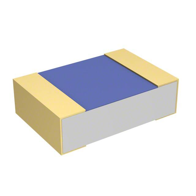
3D 3D
3D Models
For low noise and precision applications, superior stability,
low temperature coefficient of resistance, and low voltage
coefficient, Vishay Sfernice’s proven precision thin film
wraparound
resistors
exceed
requirements
of
MIL-PRF-55342G characteristics Y ± 10 ppm/°C (-55 °C;
+155 °C) down to ± 5 ppm/°C (-55 °C; +155 °C).
Note
* This datasheet provides information about parts that are
RoHS-compliant and / or parts that are non RoHS-compliant. For
example, parts with lead (Pb) terminations are not RoHS-compliant.
Please see the information / tables in this datasheet for details
STANDARD ELECTRICAL SPECIFICATIONS
MODEL
SIZE
RESISTANCE
RANGE (2)
(Ω)
RATED
POWER
W
Pn (1)
RATED
POWER
W
Pd (1)
LIMITING
ELEMENT
VOLTAGE
V
TOLERANCE
±%
TEMPERATURE
COEFFICIENT
± ppm/°C
P0302
0302
10 to 420K
0.040
0.030
25
0.01, 0.02, 0.05, 0.1, 0.25, 0.5, 1, 2, 5
5, 10, 25, 50, 100
P0402
0402
10 to 1M
0.063
0.040
50
0.01, 0.02, 0.05, 0.1, 0.25, 0.5, 1, 2, 5
5, 10, 25, 50, 100
P0505
0505
10 to 4M
0.125
0.050
50
0.01, 0.02, 0.05, 0.1, 0.25, 0.5, 1, 2, 5
5, 10, 25, 50, 100
P0603
0603
10 to 3.2M
0.125
0.100
75
0.01, 0.02, 0.05, 0.1, 0.25, 0.5, 1, 2, 5
5, 10, 25, 50, 100
P0805 (3)
0805
10 to 8M
0.200
0.125
150
0.01, 0.02, 0.05, 0.1, 0.25, 0.5, 1, 2, 5
5, 10, 25, 50, 100
P1005
1005
10 to 7.5M
0.250
0.125
75
0.01, 0.02, 0.05, 0.1, 0.25, 0.5, 1, 2, 5
5, 10, 25, 50, 100
P1206
1206
10 to 22M
0.330
0.250
200
0.01, 0.02, 0.05, 0.1, 0.25, 0.5, 1, 2, 5
5, 10, 25, 50, 100
P1505
1505
10 to 13.8M
0.350
0.175
200
0.01, 0.02, 0.05, 0.1, 0.25, 0.5, 1, 2, 5
5, 10, 25, 50, 100
P2010
2010
10 to 62M
1 (4)
0.500
300
0.01, 0.02, 0.05, 0.1, 0.25, 0.5, 1, 2, 5
5, 10, 25, 50, 100
P2512
2512
10 to 86M
2 (4)
1
300
0.01, 0.02, 0.05, 0.1, 0.25, 0.5, 1, 2, 5
5, 10, 25, 50, 100
Notes
(1) Pn = nominal power: Pd = derated power intended to improve stability
(2) For ohmic range versus tolerance and TCR see detailed table on next page
(3) Model P0805 having the same size than P0705 and the same performances, only codification of P0805 remains
(4) With special assembly care
CLIMATIC SPECIFICATIONS
MECHANICAL SPECIFICATIONS
Operating temperature
range
Substrate
Alumina
Technology
Thin film
-55 °C; +155 °C
Note
• For temperature up to 230 °C, see PHT datasheet
(www.vishay.com/doc?53050)
Film
Protection
PERFORMANCE VS. HUMID SULFUR VAPOR
Test conditions
Test results
Revision: 18-Oct-2021
50 °C ± 2 °C, 85 % ± 4 % RH,
exposure time 500 h
Resistance drift < (0.05 % R + 0.05 Ω),
no corrosion products observed
Terminations
Nickel chromium with mineral
passivation or CrSi
Epoxy + silicone
B type: SnPb over nickel barrier for
solder reflow
N type: SnAg over nickel barrier
G type: gold over nickel barrierfor
other applications
Document Number: 53017
1
For technical questions, contact: sferthinfilm@vishay.com
THIS DOCUMENT IS SUBJECT TO CHANGE WITHOUT NOTICE. THE PRODUCTS DESCRIBED HEREIN AND THIS DOCUMENT
ARE SUBJECT TO SPECIFIC DISCLAIMERS, SET FORTH AT www.vishay.com/doc?91000
�P
www.vishay.com
Vishay Sfernice
DIMENSIONS in millimeters (inches)
A
D
D
B
C
E
CASE SIZE
E
A
B
MAX. TOL.
+0.152 (+0.006)
MIN. TOL.
-0.152 (-0.006)
MAX. TOL.
+0.127 (+0.005)
MIN. TOL.
-0.127 (-0.005)
NOMINAL
NOMINAL
D/E
C
NOMINAL
TOLERANCE
0302
0.75 (0.029)
0.60 (0.024)
0.15 (0.006)
0.08 (0.003)
0402
1.00 (0.039)
0.60 (0.024)
0.25 (0.010)
0.1 (0.004)
0505
1.27 (0.005)
1.27 (0.050)
0603
1.52 (0.060)
0.85 (0.033)
0805
1.91 (0.075)
1.27 (0.050)
1005
2.54 (0.100)
1.27 (0.050)
1206
3.06 (0.120)
1.60 (0.063)
1505
3.81 (0.150)
1.32 (0.052)
2010
5.08 (0.200)
2.54 (0.100)
2512
6.30 (0.248)
3.30 (0.130)
0.38 (0.015)
0.5 (0.02)
± 0.127 (0.005)
0.40 (0.016)
0.13 (0.005)
0.48 (0.019)
0.48 (0.019)
Note
• Model P0805 having the same size than P0705 and the same performances, only codification of P0805 remains
SUGGESTED LAND PATTERN (to IPC-7351A)
Gmin.
Xmax.
Zmax.
DIMENSIONS in millimeters (inches)
CHIP SIZE
Zmax.
Gmin.
Xmax.
0302
1.30 (0.051)
0.15 (0.006)
0.73 (0.029)
0402
1.55 (0.061)
0.15 (0.006)
0.73 (0.029)
0505
1.82 (0.072)
0.10 (0.004)
1.40 (0.055)
0603
2.37 (0.093)
0.35 (0.014)
0.98 (0.039)
0805
2.76 (0.109)
0.74 (0.029)
1.40 (0.055)
1005
3.39 (0.133)
1.37 (0.054)
1.40 (0.055)
1206
3.91 (0.154)
1.85 (0.073)
1.73 (0.068)
1505
4.66 (0.183)
2.44 (0.096)
1.45 (0.057)
2010
5.93 (0.233)
3.71 (0.146)
2.67 (0.105)
2512
7.15 (0.281)
4.93 (0.194)
3.43 (0.135)
Revision: 18-Oct-2021
Document Number: 53017
2
For technical questions, contact: sferthinfilm@vishay.com
THIS DOCUMENT IS SUBJECT TO CHANGE WITHOUT NOTICE. THE PRODUCTS DESCRIBED HEREIN AND THIS DOCUMENT
ARE SUBJECT TO SPECIFIC DISCLAIMERS, SET FORTH AT www.vishay.com/doc?91000
�P
www.vishay.com
Vishay Sfernice
POWER DERATING CURVE
TCR
CODE
FILM
± 5 ppm/°C
C (-55 °C; +155 °C)
NiCr
± 5 ppm/°C
Z (0 °C; +70 °C)
NiCr
± 10 ppm/°C
Y
NiCr
± 25 ppm/°C
E
NiCr
± 50 ppm/°C
H
NiCr or CrSi
± 100 ppm/°C
K
NiCr or CrSi
Rated Power (%)
TEMPERATURE COEFFICIENT
100
80
60
40
20
0
0
20
40
60 70 80
100
120
140 155
Ambient Temperature in °C
BEST TOLERANCE AND TCR VS. OHMIC VALUE
STYLE
0302
RANGE
(Ω)
TOLERANCE
(± %)
TCR CODE
10 to < 50
0.1; 0.25; 0.5; 1; 2; 5
C; Z; Y; E; H; K
50 to < 100
0.05; 0.1; 0.25; 0.5; 1; 2; 5
C; Z; Y; E; H; K
100 to < 250
0.02; 0.05; 0.1; 0.25; 0.5; 1; 2; 5
C; Z; Y; E; H; K
250 to 30K
0.01; 0.02; 0.05; 0.1; 0.25; 0.5; 1; 2; 5
C; Z; Y; E; H; K
> 30K to 40K
0.01; 0.02; 0.05; 0.1; 0.25; 0.5; 1; 2; 5
Z; Y; E; H; K
> 40K to 65K
0.05; 0.1; 0.25; 0.5; 1; 2; 5
E; H; K
> 65K to 420K
0402
0505
0.1; 0.25; 0.5; 1; 2; 5
C; Z; Y; E; H; K
50 to < 100
0.05; 0.1; 0.25; 0.5; 1; 2; 5
C; Z; Y; E; H; K
100 to < 250
0.02; 0.05; 0.1; 0.25; 0.5; 1; 2; 5
C; Z; Y; E; H; K
250 to 67K
0.01; 0.02; 0.05; 0.1; 0.25; 0.5; 1; 2; 5
C; Z; Y; E; H; K
> 67K to 200K
0.01; 0.02; 0.05; 0.1; 0.25; 0.5; 1; 2; 5
Z; Y; E; H; K
> 200K to 341K
0.05; 0.1; 0.25; 0.5; 1; 2; 5
E; H; K
> 341K to 1M
0.1; 0.25; 0.5; 1; 2; 5 (1)
H; K
10 to < 50
0.1; 0.25; 0.5; 1; 2; 5
C; Z; Y; E; H; K
50 to < 100
0.05; 0.1; 0.25; 0.5; 1; 2; 5
C; Z; Y; E; H; K
100 to < 250
0.02; 0.05; 0.1; 0.25; 0.5; 1; 2; 5
C; Z; Y; E; H; K
250 to 187K
0.01; 0.02; 0.05; 0.1; 0.25; 0.5; 1; 2; 5
C; Z; Y; E; H; K
> 187K to 260K
0.01; 0.02; 0.05; 0.1; 0.25; 0.5; 1; 2; 5
Z; Y; E; H; K
> 260K to 400K
0.05; 0.1; 0.25; 0.5; 1; 2; 5
E; H; K
10 to < 50
0.1; 0.25; 0.5; 1; 2; 5
(1)
H; K
0.1; 0.25; 0.5; 1; 2; 5
C; Z; Y; E; H; K
50 to < 100
0.05; 0.1; 0.25; 0.5; 1; 2; 5
C; Z; Y; E; H; K
100 to < 250
0.02; 0.05; 0.1; 0.25; 0.5; 1; 2; 5
C; Z; Y; E; H; K
250 to 160K
0.01; 0.02; 0.05; 0.1; 0.25; 0.5; 1; 2; 5
C; Z; Y; E; H; K
> 160K to 332K
0.01; 0.02; 0.05; 0.1; 0.25; 0.5; 1; 2; 5
Z; Y; E; H; K
> 332K to 500K
0.05; 0.1; 0.25; 0.5; 1; 2; 5
E; H; K
> 500K to 3M2
Revision: 18-Oct-2021
H; K
10 to < 50
> 400K to 4M
0603
0.1; 0.25; 0.5; 1; 2; 5
(1)
0.1; 0.25; 0.5; 1; 2; 5
(1)
H; K
Document Number: 53017
3
For technical questions, contact: sferthinfilm@vishay.com
THIS DOCUMENT IS SUBJECT TO CHANGE WITHOUT NOTICE. THE PRODUCTS DESCRIBED HEREIN AND THIS DOCUMENT
ARE SUBJECT TO SPECIFIC DISCLAIMERS, SET FORTH AT www.vishay.com/doc?91000
�P
www.vishay.com
Vishay Sfernice
BEST TOLERANCE AND TCR VS. OHMIC VALUE
STYLE
0805
1005
1206
RANGE
(Ω)
TOLERANCE
(± %)
TCR CODE
10 to < 50
0.1; 0.25; 0.5; 1; 2; 5
C; Z; Y; E; H; K
50 to < 100
0.05; 0.1; 0.25; 0.5; 1; 2; 5
C; Z; Y; E; H; K
100 to < 250
0.02; 0.05; 0.1; 0.25; 0.5; 1; 2; 5
C; Z; Y; E; H; K
250 to 360K
0.01; 0.02; 0.05; 0.1; 0.25; 0.5; 1; 2; 5
C; Z; Y; E; H; K
> 360K to 511K
0.01; 0.02; 0.05; 0.1; 0.25; 0.5; 1; 2; 5
Z; Y; E; H; K
> 511K to 750K
0.05; 0.1; 0.25; 0.5; 1; 2; 5
E; H; K
> 750K to 8M
0.1; 0.25; 0.5; 1; 2; 5 (1)
H; K
10 to < 50
0.1; 0.25; 0.5; 1; 2; 5
C; Z; Y; E; H; K
50 to < 100
0.05; 0.1; 0.25; 0.5; 1; 2; 5
C; Z; Y; E; H; K
100 to < 250
0.02; 0.05; 0.1; 0.25; 0.5; 1; 2; 5
C; Z; Y; E; H; K
250 to 400K
0.01; 0.02; 0.05; 0.1; 0.25; 0.5; 1; 2; 5
C; Z; Y; E; H; K
> 400K to 550K
0.01; 0.02; 0.05; 0.1; 0.25; 0.5; 1; 2; 5
Z; Y; E; H; K
> 550K to 810K
0.05; 0.1; 0.25; 0.5; 1; 2; 5
E; H; K
> 810K to 7M5
0.1; 0.25; 0.5; 1; 2; 5 (1)
H; K
10 to < 50
0.1; 0.25; 0.5; 1; 2; 5
C; Z; Y; E; H; K
C; Z; Y; E; H; K
50 to < 100
0.05; 0.1; 0.25; 0.5; 1; 2; 5
100 to < 250
0.02; 0.05; 0.1; 0.25; 0.5; 1; 2; 5
C; Z; Y; E; H; K
250 to 1M3
0.01; 0.02; 0.05; 0.1; 0.25; 0.5; 1; 2; 5
C; Z; Y; E; H; K
> 1M3 to 2M
0.01; 0.02; 0.05; 0.1; 0.25; 0.5; 1; 2; 5
Z; Y; E; H; K
> 2M to 3M5
0.05; 0.1; 0.25; 0.5; 1; 2; 5
E; H; K
> 3M5 to 22M
1505
2010
H; K
10 to < 50
0.1; 0.25; 0.5; 1; 2; 5
C; Z; Y; E; H; K
50 to < 100
0.05; 0.1; 0.25; 0.5; 1; 2; 5
C; Z; Y; E; H; K
100 to < 250
0.02; 0.05; 0.1; 0.25; 0.5; 1; 2; 5
C; Z; Y; E; H; K
250 to 720K
0.01; 0.02; 0.05; 0.1; 0.25; 0.5; 1; 2; 5
C; Z; Y; E; H; K
> 720K to 1M
0.01; 0.02; 0.05; 0.1; 0.25; 0.5; 1; 2; 5
Z; Y; E; H; K
> 1M to 1M5
0.05; 0.1; 0.25; 0.5; 1; 2; 5
E; H; K
> 1M5 to 13M8
0.1; 0.25; 0.5; 1; 2; 5 (1)
H; K
10 to < 50
0.1; 0.25; 0.5; 1; 2; 5
C; Z; Y; E; H; K
50 to < 100
0.05; 0.1; 0.25; 0.5; 1; 2; 5
C; Z; Y; E; H; K
100 to < 250
0.02; 0.05; 0.1; 0.25; 0.5; 1; 2; 5
C; Z; Y; E; H; K
250 to 3M8
0.01; 0.02; 0.05; 0.1; 0.25; 0.5; 1; 2; 5
C; Z; Y; E; H; K
> 3M8 to 5M
0.01; 0.02; 0.05; 0.1; 0.25; 0.5; 1; 2; 5
Z; Y; E; H; K
> 5M to 7M5
0.05; 0.1; 0.25; 0.5; 1; 2; 5
E; H; K
> 7M5 to 62M
10 to < 50
2512
0.1; 0.25; 0.5; 1; 2; 5
(1)
0.1; 0.25; 0.5; 1; 2; 5
(1)
H; K
0.1; 0.25; 0.5; 1; 2; 5
C; Z; Y; E; H; K
C; Z; Y; E; H; K
50 to < 100
0.05; 0.1; 0.25; 0.5; 1; 2; 5
100 to < 250
0.02; 0.05; 0.1; 0.25; 0.5; 1; 2; 5
C; Z; Y; E; H; K
250 to 6M4
0.01; 0.02; 0.05; 0.1; 0.25; 0.5; 1; 2; 5
C; Z; Y; E; H; K
> 6M4 to 8M6
0.01; 0.02; 0.05; 0.1; 0.25; 0.5; 1; 2; 5
Z; Y; E; H; K
> 8M6 to 12M9
0.05; 0.1; 0.25; 0.5; 1; 2; 5
E; H; K
> 12M9 to 86M
0.1; 0.25; 0.5; 1; 2; 5 (1)
H; K
Note
(1) Tolerance 0.05 % on request
Revision: 18-Oct-2021
Document Number: 53017
4
For technical questions, contact: sferthinfilm@vishay.com
THIS DOCUMENT IS SUBJECT TO CHANGE WITHOUT NOTICE. THE PRODUCTS DESCRIBED HEREIN AND THIS DOCUMENT
ARE SUBJECT TO SPECIFIC DISCLAIMERS, SET FORTH AT www.vishay.com/doc?91000
�P
www.vishay.com
Vishay Sfernice
POPULAR OPTIONS
For any option it is recommended to consult Vishay Sfernice for availability first.
Option: Enlarged Terminations
For stringent and special power dissipation requirements, the thermal resistance between the resistive layer and the solder joint
can be reduced using enlarged terminations chip resistors which are soldered on large and thick copper pads acting as heatsink
(see application note: 53048 Power Dissipation in High Precision Vishay Sfernice Chip Resistors and Arrays (P Thin Film, PRA
Arrays, CHP Thick Film) www.vishay.com/doc?53048.
Option to order 0063: (applies to size 1206 / 1505 / 2010 / 2512).
DIMENSIONS (Option 0063) in millimeters
Bottom view for mounting
Uncoatted
ceramic
A
Enlarged
termination
B
F
D
D
E
CASE SIZE
E
A
B
E
D
MAX. TOL.
+0.152
MIN. TOL.
-0.152
MAX. TOL.
+0.127
MIN. TOL.
-0.127
MAX. TOL.
+0.13
MIN. TOL.
-0.13
MAX. TOL.
+0.13
MIN. TOL.
-0.13
NOMINAL
NOMINAL
NOMINAL
NOMINAL
1206
3.06
1.60
0.40
1.215
1505
3.81
1.32
2010
5.08
2.54
2512
6.30
3.30
1.59
0.48
2.215
F
NOMINAL
MIN.
MAX.
0.63
0.50
0.76
2.835
SUGGESTED LAND PATTERN (Option 0063)
Gmin.
Xmax.
Zmax.
CHIP SIZE
DIMENSIONS (IN MILLIMETER)
Zmax.
1206
3.91
1505
4.66
2010
5.93
2512
7.15
Revision: 18-Oct-2021
Gmin.
Xmax.
1.73
0.50
1.45
2.67
3.43
Document Number: 53017
5
For technical questions, contact: sferthinfilm@vishay.com
THIS DOCUMENT IS SUBJECT TO CHANGE WITHOUT NOTICE. THE PRODUCTS DESCRIBED HEREIN AND THIS DOCUMENT
ARE SUBJECT TO SPECIFIC DISCLAIMERS, SET FORTH AT www.vishay.com/doc?91000
�P
www.vishay.com
Vishay Sfernice
Option: Marking
Option to order 0013:
Marking of ohmic value and tolerance:
Sizes: 0805 to 1005: 3 digits marking (according to EIA-96)
Sizes: 1206 to 2512: 4 digits marking (same codification than in the ordering procedure)
Tolerance indicated by a color dot.
Option to order 0014:
Marking of ohmic value:
Sizes: 0805 to 1005: 3 digits marking (according to EIA-96)
Sizes: 1206 to 2512: 4 digits marking (same codification than in the ordering procedure)
No standard marking available for smaller sizes.
A price adder will apply to the unit price of the parts for options 0013 and 0014.
Option: AEC-Q200
For moisture resistance test only.
Option to Order 0058:
Specific production process to withstand 85 °C/85 % at Pn/10
PACKAGING
PACKAGING RULES
ESD packaging available: waffle-pack and plastic tape and
reel (low conductivity). Paper tape available upon request
(for sizes 0402, 0603, 0805 and 1206).
Waffle Pack
SIZE MOQ
0302
0402
0505
0603
0805
1005
1206
1505
2010
2512
NUMBER OF PIECES PER PACKAGE
TAPE
TAPE AND REEL
WAFFLE PACK
WIDTH
2" × 2"
MIN.
MAX.
250
100
340
5000
100
4000
5000
221
140
60
50
8 mm
100
4000
1000
2000
Can be filled up to maximum quantity indicated in the table
here above, taking into account the minimum order quantity.
When quantity ordered exceeds maximum quantity of a
single waffle pack, the waffle packs are stacked up on the
top of each other and closed by one single cover.
To get “not stacked up” waffle pack in case of ordered
quantity > maximum number of pieces per package:
Please consult Vishay Sfernice for specific ordering
code.
Tape and Reel
See Part Numbering information to get the quantity desired
by tape.
12 mm
PERFORMANCE
TESTS
Thermal shock
Short time overload
Low temperature operation
Resistance to solder heat
Moisture resistance
High temperature
Load life
CONDITIONS
MIL-PRF-55342G
MIL-STD-202 F-Method 107 F
MIL-PRF-55342G
PARA 3.10.4.7.5
MIL-PRF-55342G
PARA 3.9 and 4.7.4
MIL-PRF-55342G
PARA 3.12, 4.7.7, 4.7.1.2
MIL-PRF-55342G
PARA 3.13 and 4.7.8
MIL-STD-202 F-Method 106 E
CECC 56 days/40 °C/93 % RH
AEC-Q200 (1)
85 °C/85 % RH/Pn/10, 1000 h
MIL-PRF-55342G
PARA 3.11 and 4.7.6
MIL-PRF-55342G
8000 h Pn at 70 °C
MIL-STD-202 F-Method 108 A
MIL OR CECC
REQUIREMENTS
TYPICAL
PERFORMANCES
± 0.05 %
± 0.02 %
± 0.05 %
± 0.01 %
± 0.05 %
± 0.01 %
± 0.05 %
± 0.03 %
± 0.10 %
± 0.01 %
± 0.10 %
± 0.01 %
± 0.5 % + 0.05 Ω
Max. < 0.3 % + 0.05 Ω
± 0.05 %
± 0.05 %
± 0.5 %
± 0.1 % (2)
Notes
(1) Option to order 0058
(2) Typical drift ± 0.02 % at Pd
Revision: 18-Oct-2021
Document Number: 53017
6
For technical questions, contact: sferthinfilm@vishay.com
THIS DOCUMENT IS SUBJECT TO CHANGE WITHOUT NOTICE. THE PRODUCTS DESCRIBED HEREIN AND THIS DOCUMENT
ARE SUBJECT TO SPECIFIC DISCLAIMERS, SET FORTH AT www.vishay.com/doc?91000
�P
www.vishay.com
Vishay Sfernice
Maximum permissible pulse load Pi max. for single pulse (1)
Permissible Pulse Power P (W)
100
P2512
P2010
P1206
P0805
P0603
P0402
10
1
0.1
0.00001
0.0001
0.001
0.01
0.1
1
10
Pulse Duration t (s)
Energy for single pulse (1)
100
Permissible Pulse Energy (J)
10
1
0.1
0.01
P2512
P2010
P1206
P0805
P0603
P0402
0.001
0.0001
0.00001
0.00001
0.0001
0.001
0.01
0.1
1
10
Pulse Duration t (s)
Maximum permissible pulse voltage Ui max. for single pulse (1)
Permissible Pulse Voltage (V)
10 000
P2512
P2010
P1206
P0805
P0603
P0402
1000
100
10
0.00001
0.0001
0.001
0.01
0.1
1
10
Pulse Duration t (s)
Note
(1) One should apply the data mentioned on the 3 curves together to get the right performances
Revision: 18-Oct-2021
Document Number: 53017
7
For technical questions, contact: sferthinfilm@vishay.com
THIS DOCUMENT IS SUBJECT TO CHANGE WITHOUT NOTICE. THE PRODUCTS DESCRIBED HEREIN AND THIS DOCUMENT
ARE SUBJECT TO SPECIFIC DISCLAIMERS, SET FORTH AT www.vishay.com/doc?91000
�P
www.vishay.com
Vishay Sfernice
Maximum permissible pulse load Pi max.
Permissible Pulse Power P (W)
100
P2512
P2010
P1206
P0805
P0603
P0402
10
1
0.1
0.00001
0.0001
0.001
0.01
0.1
1
10
Pulse Duration t (s)
1.2/50 μs lightning surge
Test Voltage (V)
10 000
1000
100
P2512
P1206
P0805
P0603
10
10
100
1000
10 000
100 000
Resistor Value (Ω)
10/700 μs lightning surge
Test Voltage (V)
10 000
1000
100
P2512
P2010
P1206
P0805
P0603
10
10
100
1000
10 000
100 000
Resistor Value (Ω)
Revision: 18-Oct-2021
Document Number: 53017
8
For technical questions, contact: sferthinfilm@vishay.com
THIS DOCUMENT IS SUBJECT TO CHANGE WITHOUT NOTICE. THE PRODUCTS DESCRIBED HEREIN AND THIS DOCUMENT
ARE SUBJECT TO SPECIFIC DISCLAIMERS, SET FORTH AT www.vishay.com/doc?91000
�P
www.vishay.com
Vishay Sfernice
GLOBAL PART NUMBER INFORMATION
New Global Part Numbering: P0505Y1003BBT0999
P
0
5
0
5
Y
1
0
0
3
B
B
T
9
9
9
GLOBAL MODEL
SIZE
TCR
VALUE
TOLERANCE
TERMINATION
PACKAGING
OPTION
P
0302
0402
0505
0603
0805
1005
1206
1505
2010
2512
K = ± 100 ppm/°C
H = ± 50 ppm/°C
E = ± 25 ppm/°C
Y = ± 10 ppm/°C
Z = ± 5 ppm
(0 °C; +70 °C)
C = ± 5 ppm
(- 55 °C; + 155 °C)
The first three digits
are significant figures
and the last digit
specifies the number
of zeros to follow,
R designates
decimal point
L = ± 0.01 %
P = ± 0.02 %
W = ± 0.05 %
B = ± 0.1 %
C = ± 0.25 %
D = ± 0.5 %
F=±1%
G=±2%
J=±5%
B: SnPb over
nickel barrier
N: SnAg over
nickel barrier
G: gold over
nickel barrier
For more
information
see
“Codification
of
packaging”
table
From 1 to 3
digits, leave
blank if
no option
10R0 = 10 Ω
3901 = 3900 Ω
1004 = 1 MΩ
B: lead bearing version
N and G: lead (Pb)-free/RoHS version
Historical Part Number Examples:
P1206Y1001LNT100 (tapes of 100 pieces)
P1206H7151FBT250 (tapes of 250 pieces)
P1206Y1503WNT1K032 (tapes of 1000 pieces and option 32)
P1206Y2372BG (waffle pack)
Historical part numbers are not recommended, but can still be used for ordering.
CODIFICATION OF PACKAGING
CODE 18
PACKAGING
WAFFLE PACK
W
100 min., 1 mult.
WA
100 min., 100 mult. (available only in size 1206)
PLASTIC TAPE (in standard for all sizes)
T
100 min., 1 mult.
TA
100 min., 100 mult.
TB
250 min., 250 mult.
TC
500 min., 500 mult.
TD
1000 min., 1000 mult.
TE
2500 min., 2500 mult.
TF
Full tape (quantity depending on size of chips)
PAPER TAPE (available for 0402, 0603, 0805, and 1206. Please consult Vishay Sfernice for other sizes)
PT
100 min., 1 mult.
PA
100 min., 100 mult.
PB
250 min., 250 mult.
PC
500 min., 500 mult.
PD (not available for size 0402)
1000 min., 1000 mult.
PE (not available for size 0402)
2500 min., 2500 mult.
PF (not available for size 0402)
Full tape (quantity depending on size of chips)
Notes
• For CECC qualified, see RV datasheet (www.vishay.com/doc?60022)
• For ESCC qualified, see PHR datasheet (www.vishay.com/doc?53037) or PFRR datasheet (www.vishay.com/doc?53046)
• For high temperature (230 °C), see PHT datasheet (www.vishay.com/doc?53050)
• For very high temperature (270 °C), see PVHT datasheet (www.vishay.com/doc?53060)
• For strap (0 Ω), see PZR datasheet (www.vishay.com/doc?53053)
Revision: 18-Oct-2021
Document Number: 53017
9
For technical questions, contact: sferthinfilm@vishay.com
THIS DOCUMENT IS SUBJECT TO CHANGE WITHOUT NOTICE. THE PRODUCTS DESCRIBED HEREIN AND THIS DOCUMENT
ARE SUBJECT TO SPECIFIC DISCLAIMERS, SET FORTH AT www.vishay.com/doc?91000
�Legal Disclaimer Notice
www.vishay.com
Vishay
Disclaimer
ALL PRODUCT, PRODUCT SPECIFICATIONS AND DATA ARE SUBJECT TO CHANGE WITHOUT NOTICE TO IMPROVE
RELIABILITY, FUNCTION OR DESIGN OR OTHERWISE.
Vishay Intertechnology, Inc., its affiliates, agents, and employees, and all persons acting on its or their behalf (collectively,
“Vishay”), disclaim any and all liability for any errors, inaccuracies or incompleteness contained in any datasheet or in any other
disclosure relating to any product.
Vishay makes no warranty, representation or guarantee regarding the suitability of the products for any particular purpose or
the continuing production of any product. To the maximum extent permitted by applicable law, Vishay disclaims (i) any and all
liability arising out of the application or use of any product, (ii) any and all liability, including without limitation special,
consequential or incidental damages, and (iii) any and all implied warranties, including warranties of fitness for particular
purpose, non-infringement and merchantability.
Statements regarding the suitability of products for certain types of applications are based on Vishay's knowledge of typical
requirements that are often placed on Vishay products in generic applications. Such statements are not binding statements
about the suitability of products for a particular application. It is the customer's responsibility to validate that a particular product
with the properties described in the product specification is suitable for use in a particular application. Parameters provided in
datasheets and / or specifications may vary in different applications and performance may vary over time. All operating
parameters, including typical parameters, must be validated for each customer application by the customer's technical experts.
Product specifications do not expand or otherwise modify Vishay's terms and conditions of purchase, including but not limited
to the warranty expressed therein.
Hyperlinks included in this datasheet may direct users to third-party websites. These links are provided as a convenience and
for informational purposes only. Inclusion of these hyperlinks does not constitute an endorsement or an approval by Vishay of
any of the products, services or opinions of the corporation, organization or individual associated with the third-party website.
Vishay disclaims any and all liability and bears no responsibility for the accuracy, legality or content of the third-party website
or for that of subsequent links.
Except as expressly indicated in writing, Vishay products are not designed for use in medical, life-saving, or life-sustaining
applications or for any other application in which the failure of the Vishay product could result in personal injury or death.
Customers using or selling Vishay products not expressly indicated for use in such applications do so at their own risk. Please
contact authorized Vishay personnel to obtain written terms and conditions regarding products designed for such applications.
No license, express or implied, by estoppel or otherwise, to any intellectual property rights is granted by this document or by
any conduct of Vishay. Product names and markings noted herein may be trademarks of their respective owners.
© 2021 VISHAY INTERTECHNOLOGY, INC. ALL RIGHTS RESERVED
Revision: 09-Jul-2021
1
Document Number: 91000
�


 工商网监
湘ICP备2023018690号
工商网监
湘ICP备2023018690号
