PCAN
www.vishay.com
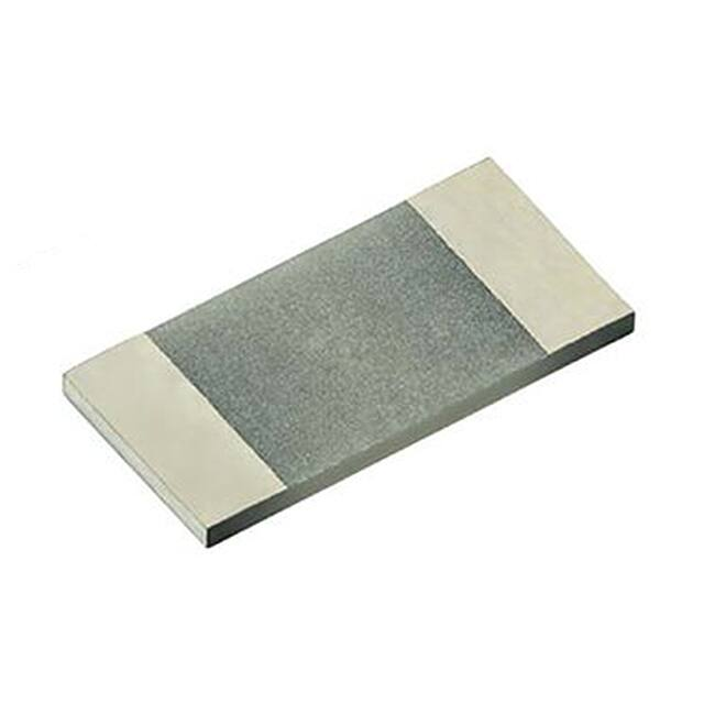
Vishay Dale Thin Film
High Power Aluminum Nitride, Wraparound Surface Mount,
Precision Thin Film Chip Resistor (Up to 6 W)
FEATURES
• High thermal conductivity aluminum nitride
substrate
Available
• Power rating up to 6.0 W
Available
• Resistance range 2 Ω to 30.1 kΩ
• Resistor tolerance to ± 0.1 %
• TCR to ± 25 ppm/°C
• Flame resistant UL 94 V-0
Available
• Material categorization: for definitions of
compliance please see www.vishay.com/doc?99912
LINKS TO ADDITIONAL RESOURCES
3D 3D
3D Models
Note
* This datasheet provides information about parts that are
RoHS-compliant and / or parts that are non RoHS-compliant. For
example, parts with lead (Pb) terminations are not RoHS-compliant.
Please see the information / tables in this datasheet for details
APPLICATIONS
Infographics
PCAN series chip resistors are designed on aluminum
nitride ceramic substrates with enlarged backside
terminations to reduce the thermal resistance between the
topside resistor layer and the solder joint on the end users
circuit assembly.
Actual power handling capability is limited by the end user
mounting process. As with any high power chip resistor the
ability to remove the heat is critical to the overall
performance of the device.
• Power supplies
• Power switching
• Braking system
TYPICAL PERFORMANCE
ABSOLUTE
TCR
25
TOL.
0.1
STANDARD ELECTRICAL SPECIFICATIONS
TEST
Material
Resistance Range
TCR: Absolute
Tolerance: Absolute
Power Rating: Resistor
Stability: Absolute
Voltage Coefficient
Working Voltage
Operating Temperature Range
Storage Temperature Range
Noise
Shelf Life Stability: Absolute
SPECIFICATIONS
Passivated nichrome
2 Ω to 30.1 kΩ
25 ppm/°C (standard) and 100 ppm/°C
0.1 %, 0.25 %, 0.5 %, 1.0 %, 2.0 %, and 5.0 %
0.5 W to 6.0 W (1)
ΔR 1.0 %
< 0.1 ppm/V
75 V to 100 V
-55 °C to +155 °C
-55 °C to +155 °C
< -30 dB
± 0.01 %
CONDITIONS
-55 °C to +150 °C
Maximum at +70 °C
1000 h at +70 °C
1 year at +25 °C
Note
(1) Dependant on component mounting by user
COMPONENT RATINGS
CASE SIZE
0603
0805
1206
2512
POWER RATING (mW)
500 (1)
1000 (1)
2000 (1)
6000 (1)
WORKING VOLTAGE (V)
75
100
100
100
RESISTANCE RANGE (Ω)
2 to 30.1K
2 to 30.1K
2 to 30.1K
2 to 30.1K
Note
Dependant on component mounting by user
(1)
Revision: 08-Mar-2021
Document Number: 60125
1
For technical questions, contact: thinfilm@vishay.com
THIS DOCUMENT IS SUBJECT TO CHANGE WITHOUT NOTICE. THE PRODUCTS DESCRIBED HEREIN AND THIS DOCUMENT
ARE SUBJECT TO SPECIFIC DISCLAIMERS, SET FORTH AT www.vishay.com/doc?91000
�PCAN
www.vishay.com
Vishay Dale Thin Film
ENVIRONMENTAL TESTS
ENVIRONMENTAL TEST (1)
TEST LIMITS
TYPICAL VISHAY
PERFORMANCE
Resistance temperature characteristic
± 25 ppm/°C
± 15 ppm/°C
Maximum ambient temperature at rated wattage
+70 °C
+70 °C
Maximum ambient temperature at power derating
+150 °C
+150 °C
Thermal shock
± 0.25 %
± 0.10 %
Low temperature operation
± 0.25 %
± 0.01 %
Short time overload
± 0.5 %
± 0.2 %
High temperature exposure
± 0.2 %
± 0.05 %
Resistance to soldering heat
± 0.25 %
± 0.025 %
Moisture resistance
± 0.4 %
± 0.01 %
Life at +70 °C for 1000 h
± 1.00 %
± 0.4 %
Note
(1) Environmental testing was performed based on MIL-STD-202 standard test methods
DIMENSIONS in inches
D
T
D
W
T
E
L
L
LENGTH
L
WIDTH
W
THICKNESS
T
MIN. / MAX.
TOP PAD
D
BOTTOM PAD
E
0603
0.064 ± 0.006
0.032 ± 0.005
0.015 ± 0.003
0.012 ± 0.005
0.021 ± 0.005
0805
0.080 ± 0.006
0.050 ± 0.005
0.015 ± 0.003
0.016 ± 0.005
0.025 ± 0.005
1206
0.126 ± 0.008
0.063 ± 0.005
0.015 ± 0.003
0.020 + 0.005 / - 0.010
0.040 ± 0.005
2512
0.259 + 0.009 / - 0.015
0.124 ± 0.005
0.015 ± 0.003
0.020 ± 0.005
0.050 ± 0.005
CASE SIZE
LAND PATTERN DIMENSIONS in inches
0603 Land Pattern
1206 Land Pattern
0.0920
0.1730
0.0340
0.0710
0.0140
0.0390
0.0220
0.0755
0805 Land Pattern
2512 Land Pattern
0.1050
0.2910
0.0520
0.1260
0.0200
0.0425
0.1090
0.0910
Revision: 08-Mar-2021
Document Number: 60125
2
For technical questions, contact: thinfilm@vishay.com
THIS DOCUMENT IS SUBJECT TO CHANGE WITHOUT NOTICE. THE PRODUCTS DESCRIBED HEREIN AND THIS DOCUMENT
ARE SUBJECT TO SPECIFIC DISCLAIMERS, SET FORTH AT www.vishay.com/doc?91000
�PCAN
www.vishay.com
Vishay Dale Thin Film
STANDARD MATERIAL SPECIFICATIONS
Resistive element
Passivated nichrome
Substrate material
Aluminum nitride
Terminations (tin/lead)
Terminations (lead (Pb)-free)
Tin / lead solder over nickel barrier
Tin / silver / copper (Sn96.5 / Ag3.0 / Cu0.5) solder over nickel barrier
PCAN0603 CHIP TEMP VS. APPLIED POWER
PCAN0805 CHIP TEMP VS. APPLIED POWER
7.0
8.0
5.0
7.0
200 Ω
6.0
Applied Power (W)
Applied Power (W)
6.0
20 Ω
4.0
3.0
2.0
200 Ω
5.0
4.0
3.0
2.0
1.0
0.0
50 Ω
1.0
70
150
Chip Surface Temperature Temperature (°C)
0.0
200
70
150
Chip Surface Temperature Temperature (°C)
200
Note
• Chip surface temperature measured using FLIR SC645 thermal
imaging system with an approximate testcard surface
temperature of 75 °C
Note
• Chip surface temperature measured using FLIR SC645 thermal
imaging system with an approximate testcard surface
temperature of 75 °C
PCAN1206 CHIP TEMP VS. APPLIED POWER
PCAN2512 CHIP TEMP VS. APPLIED POWER
12.0
12.0
8.0
175 Ω
6.0
4.0
2.0
0.0
10.0
30 Ω
Applied Power (W)
Applied Power (W)
10.0
30 Ω
150 Ω
8.0
6.0
4.0
2.0
70
150
Chip Surface Temperature Temperature (°C)
200
Note
• Chip surface temperature measured using FLIR SC645 thermal
imaging system with an approximate test card surface
temperature of 85 °C
• Thermal imaging was conducted under ambient conditions
resulting in a steady state test card surface temperature of 85 °C
over the full range of power levels
• Thermal imaging and load life testing was conducted mounting
one device to a 1.6" x 3.7" test card with 3.5 mil copper plating
on both surfaces. Thermal vias on 50 mil centers were utilized for
heat transfer between surfaces of the test card
Revision: 08-Mar-2021
0.0
70
150
Chip Surface Temperature Temperature (°C)
200
Note
• Chip surface temperature measured using FLIR SC645 thermal
imaging system with an approximate test card surface
temperature of 85 °C
Document Number: 60125
3
For technical questions, contact: thinfilm@vishay.com
THIS DOCUMENT IS SUBJECT TO CHANGE WITHOUT NOTICE. THE PRODUCTS DESCRIBED HEREIN AND THIS DOCUMENT
ARE SUBJECT TO SPECIFIC DISCLAIMERS, SET FORTH AT www.vishay.com/doc?91000
�PCAN
www.vishay.com
Vishay Dale Thin Film
DERATING CURVE
Percent of Rated Power
100
80
60
40
20
0
0
70
125
155
Ambient Temperature °C
SINGLE PULSE LOAD TESTING
100 Ω - 2512
10
100 Ω - 1206
Peak Power (W)
100
1
0.1
0.00001
0.0001
0.001
0.01
0.1
1
10
Pulse Duration (s)
GLOBAL PART NUMBER INFORMATION
New Global Part Numbering: PCAN1206H1000BBT1
P
C
A
N
1
GLOBAL
MODEL
CASE
SIZE
TCR
CHARACTERISTIC
PCAN
0603
0805
1206
2512
E = ± 25 ppm/°C
H = ± 50 ppm/°C
K = ± 100 ppm/°C (1)
2
0
6
H
1
RESISTANCE
TOLERANCE
The first 3 digits are
significant figures and
the last digit specifies
the number of zeros
to follow.
“R” designates the
decimal point.
B = ± 0.1 % (2)
C = ± 0.25 %
D = ± 0.5 %
F = ± 1.0 % (1)
G = ± 2.0 %
J = ± 5.0 %
Example:
10R0 = 10 Ω
1000 = 100 Ω
0
0
0
TERMINATION
B = wraparound
Sn/Pb solder
w/ nickel barrier
S = wraparound
lead (Pb)-free
solder (e1)
RoHS compliant
G = wraparound Au,
over Ni (gold)
termination
epoxy bondable
RoHS compliant
(e4)
B
B
T
1
PACKAGING
BS = BULK
100 min., 1 mult.
WS = WAFFLE
100 min., 1 mult.
W0 = 100 pc min. waffle,
1 mult.
WI = 100 min., 1 mult.
(package unit single lot
date code)
TAPE AND REEL
T0 = 100 min., 100 mult.
T1 = 1000 min., 1000 mult.
T3 = 300 min., 300 mult.
T5 = 500 min., 500 mult.
TF = full reel
TS = 100 min., 1 mult.
TI = 100 min., 1 mult.
(item single lot date code)
TP = 100 min., 1 mult.
(package unit single lot
date code)
Notes
(1) Less than 10 Ω. 100 ppm/°C and 1 % tolerance best
(2) Available on 10 Ω and higher
Revision: 08-Mar-2021
Document Number: 60125
4
For technical questions, contact: thinfilm@vishay.com
THIS DOCUMENT IS SUBJECT TO CHANGE WITHOUT NOTICE. THE PRODUCTS DESCRIBED HEREIN AND THIS DOCUMENT
ARE SUBJECT TO SPECIFIC DISCLAIMERS, SET FORTH AT www.vishay.com/doc?91000
�Legal Disclaimer Notice
www.vishay.com
Vishay
Disclaimer
ALL PRODUCT, PRODUCT SPECIFICATIONS AND DATA ARE SUBJECT TO CHANGE WITHOUT NOTICE TO IMPROVE
RELIABILITY, FUNCTION OR DESIGN OR OTHERWISE.
Vishay Intertechnology, Inc., its affiliates, agents, and employees, and all persons acting on its or their behalf (collectively,
“Vishay”), disclaim any and all liability for any errors, inaccuracies or incompleteness contained in any datasheet or in any other
disclosure relating to any product.
Vishay makes no warranty, representation or guarantee regarding the suitability of the products for any particular purpose or
the continuing production of any product. To the maximum extent permitted by applicable law, Vishay disclaims (i) any and all
liability arising out of the application or use of any product, (ii) any and all liability, including without limitation special,
consequential or incidental damages, and (iii) any and all implied warranties, including warranties of fitness for particular
purpose, non-infringement and merchantability.
Statements regarding the suitability of products for certain types of applications are based on Vishay's knowledge of typical
requirements that are often placed on Vishay products in generic applications. Such statements are not binding statements
about the suitability of products for a particular application. It is the customer's responsibility to validate that a particular product
with the properties described in the product specification is suitable for use in a particular application. Parameters provided in
datasheets and / or specifications may vary in different applications and performance may vary over time. All operating
parameters, including typical parameters, must be validated for each customer application by the customer's technical experts.
Product specifications do not expand or otherwise modify Vishay's terms and conditions of purchase, including but not limited
to the warranty expressed therein.
Hyperlinks included in this datasheet may direct users to third-party websites. These links are provided as a convenience and
for informational purposes only. Inclusion of these hyperlinks does not constitute an endorsement or an approval by Vishay of
any of the products, services or opinions of the corporation, organization or individual associated with the third-party website.
Vishay disclaims any and all liability and bears no responsibility for the accuracy, legality or content of the third-party website
or for that of subsequent links.
Except as expressly indicated in writing, Vishay products are not designed for use in medical, life-saving, or life-sustaining
applications or for any other application in which the failure of the Vishay product could result in personal injury or death.
Customers using or selling Vishay products not expressly indicated for use in such applications do so at their own risk. Please
contact authorized Vishay personnel to obtain written terms and conditions regarding products designed for such applications.
No license, express or implied, by estoppel or otherwise, to any intellectual property rights is granted by this document or by
any conduct of Vishay. Product names and markings noted herein may be trademarks of their respective owners.
© 2021 VISHAY INTERTECHNOLOGY, INC. ALL RIGHTS RESERVED
Revision: 09-Jul-2021
1
Document Number: 91000
�