物料型号:VISHAY PLZ系列
器件简介:这是一系列允许500毫瓦功率耗散的硅平面齐纳二极管,具有超小型的AUTOMOTIVE可用eSMP®系列,符合RoHS标准,无卤素,并且有低轮廓MicroSMF (DO-219AC)封装。
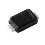
引脚分配:文档中没有提供具体的引脚分配图,但提到了器件使用MicroSMF(DO-219AC)封装。
参数特性:
- 齐纳电压范围:2.0V至39V
- 测试电流:5至20毫安
- 电路配置:单路
- 功率耗散:在不同条件下,功率耗散的值不同,例如在85°C环境温度下,安装在FR4板上的功率耗散为500毫瓦。
功能详解:文档提供了详细的电气特性,包括正向电压、反向电流、动态电阻、峰值脉冲电流、反向钳位电压和ESD抗扰度等。
应用信息:适用于汽车电子、工业级和AEC-Q101认证的电子应用。
封装信息:MicroSMF(DO-219AC)封装,重量为4.8毫克,阻燃等级为UL 94V-0,湿度敏感等级为MSL 1级,焊接条件为260°C/10秒。