RCC e3
www.vishay.com
Vishay
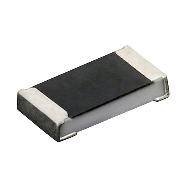
Medium Power Thick Film Chip Resistors
FEATURES
• Increased power rating
• Increased operating voltage
• AEC-Q200 qualified
• Material categorization: for definitions of
compliance please see www.vishay.com/doc?99912
APPLICATIONS
LINKS TO ADDITIONAL RESOURCES
• Automotive
3D 3D
• Industrial
• Telecommunications
3D Models
The medium power thick film chip resistor series feature a
higher power rating and operating voltage as compared to
standard chip resistors, offering the capability to replace
standard resistors of the next larger size.
• Medical
TECHNICAL SPECIFICATIONS
DESCRIPTION
RCC0402 e3
RCC0603 e3
RCC0805 e3
RCC1206 e3
0402
0603
0805
1206
RR1005M
RR1608M
RR2012M
Imperial size
Metric size code
1 to 10 M; jumper (0
Resistance range
Resistance tolerance
RR3216M
1 to 1 M;
jumper (0
± 5 %; ± 1 %
Temperature coefficient
± 200 ppm/K; ± 100 ppm/K
Rated dissipation, P70 (1)
0.125 W
0.2 W
75 V
150 V
Operating voltage, Umax. ACRMS/DC
Permissible film temperature, F max. (1)
0.25 W
0.5 W
200 V
200 V
155 °C
Operating temperature range
-55 °C to +155 °C
Max. resistance change at P70 for resistance
range, |R/R| after (2):
1000 h
3.0 %
1.0 %
8000 h
-
2.0 %
Permissible voltage against ambient
(insulation):
1 min, Uins
Failure rate: FITobserved
100 V
200 V
300 V
300 V
0.1 x 10⁻⁹/h
Notes
(1) Please refer to APPLICATION INFORMATION below
(2) Apply to components with stability class 1
APPLICATION INFORMATION
When the resistor dissipates power, a temperature rise above the ambient temperature occurs, dependent on the thermal
resistance of the assembled resistor together with the printed circuit board. The rated dissipation applies only if the permitted
film temperature is not exceeded.
These resistors do not feature a limited lifetime when operated within the permissible limits. However, resistance value drift
increasing over operating time may result in exceeding a limit acceptable to the specific application, thereby establishing a
functional lifetime.
Revision: 23-Apr-2021
Document Number: 20066
1
For technical questions, contact: thickfilmchip@vishay.com
THIS DOCUMENT IS SUBJECT TO CHANGE WITHOUT NOTICE. THE PRODUCTS DESCRIBED HEREIN AND THIS DOCUMENT
ARE SUBJECT TO SPECIFIC DISCLAIMERS, SET FORTH AT www.vishay.com/doc?91000
�RCC e3
www.vishay.com
Vishay
TEMPERATURE COEFFICIENT AND RESISTANCE RANGE
TYPE / SIZE
TCR
± 200 ppm/K
± 100 ppm/K
Jumper, Imax. = 2 A
± 200 ppm/K
± 100 ppm/K
Jumper, Imax. = 3 A
± 200 ppm/K
± 100 ppm/K
Jumper, Imax. = 3.5 A
± 200 ppm/K
± 100 ppm/K
Jumper, Imax. = 5 A
RCC0402 e3
RCC0603 e3
RCC0805 e3
RCC1206 e3
TOLERANCE
±5%
±1%
20 m
±5%
±1%
20 m
±5%
±1%
20 m
±5%
±1%
20 m
RESISTANCE
1 to 10 M
1 to 10 M
0
1 to 10 M
1 to 10 M
0
1 to 10 M
1 to 10 M
0
1 to 1 M
1 to 1 M
0
E-SERIES
E24
E24; E96
E24
E24; E96
E24
E24; E96
E24
E24; E96
-
Note
• The temperature coefficient of resistance (TCR) is not specified for 0 jumpers
PACKAGING
TYPE / SIZE
RCC0402 e3
RCC0603 e3
RCC0805 e3
RCC1206 e3
CODE
QUANTITY
ED = ET7
EE = EF4
EI = ET2
ED = ET3
EL = ET4
EE = ET8
EA = ET1
EB = ET5
EC = ET6
EA = ET1
EB = ET5
EC = ET6
EA = ET1
EB = ET5
EC = ET6
10 000
50 000
5000
10 000
20 000
50 000
5000
10 000
20 000
5000
10 000
20 000
5000
10 000
20 000
PACKAGING STYLE
WIDTH
PACKAGING
DIMENSIONS
Ø 180 mm / 7"
Ø 330 mm / 13"
Ø 180 mm / 7"
Ø 180 mm / 7"
Ø 285 mm / 11.25"
Ø 330 mm / 13"
Ø 180 mm / 7"
Ø 285 mm / 11.25"
Ø 330 mm / 13"
Ø 180 mm / 7"
Ø 285 mm / 11.25"
Ø 330 mm / 13"
Ø 180 mm / 7"
Ø 285 mm / 11.25"
Ø 330 mm / 13"
PITCH
2 mm
2 mm
Paper tape according to
IEC 60286-3, Type 1a
4 mm
8 mm
4 mm
4 mm
PART NUMBER AND PRODUCT DESCRIPTION
Part Number: RCC06031K00FKEA
Part Number: RCC06030000Z0EA
R
C
C
0
6
0
3
1
K
0
0
F
K
E
TYPE / SIZE
RESISTANCE
TOLERANCE
TCR
PACKAGING
RCC0402
RCC0603
RCC0805
RCC1206
R = decimal
K = thousand
M = million
0000 = jumper
F = ± 1.0 %
J = ± 5.0 %
Z = jumper
K = ± 100 ppm/K
N = ± 200 ppm/K
0 = jumper
EA, EB,
EC, ED,
EE, EI,
EL
A
Product Description: RCC0603 100 1K 1 % ET1 e3
Product Description: RCC0603 0R0 ET1 e3
RCC0603
100
1K
1%
ET1
e3
TYPE / SIZE
TCR
RESISTANCE
TOLERANCE
PACKAGING
LEAD (Pb)-FREE
RCC0402
RCC0603
RCC0805
RCC1206
± 100 ppm/K
± 200 ppm/K
10R = 10
100R = 100
10K = 10 k
1M0 = 1 M
0R0 = jumper
± 1.0 %
± 5.0 %
ET1, ET2,
ET3, ET4,
ET5, ET6,
ET7, ET8
EF4
e3 = pure tin
termination finish
Revision: 23-Apr-2021
Document Number: 20066
2
For technical questions, contact: thickfilmchip@vishay.com
THIS DOCUMENT IS SUBJECT TO CHANGE WITHOUT NOTICE. THE PRODUCTS DESCRIBED HEREIN AND THIS DOCUMENT
ARE SUBJECT TO SPECIFIC DISCLAIMERS, SET FORTH AT www.vishay.com/doc?91000
�RCC e3
www.vishay.com
DESCRIPTION
Production is strictly controlled and follows an extensive set
of instructions established for reproducibility. A cermet film
layer and a glass-over are deposited on a high grade (AI2O3)
ceramic substrate with its prepared inner contacts on both
sides. A special laser is used to achieve the target value and
the desired power dissipation performance by smoothly fine
trimming the resistive layer without damaging the ceramics.
The resistor elements are covered by a protective coating
designed for electrical, mechanical and climatic protection.
The terminations receive a final pure tin on nickel plating.
The result of the determined production is verified by an
extensive testing procedure on 100 % of the individual chip
resistors. Only accepted products are laid directly into the
tape in accordance with IEC 60286-3 Type 1a (1).
ASSEMBLY
The resistors are suitable for processing on automatic SMD
assembly systems. They are suitable for automatic
soldering using wave, reflow or vapor phase as shown in
IEC 61760-1. The encapsulation is resistant to all cleaning
solvents commonly used in the electronics industry,
including alcohols, esters and aqueous solutions. The
suitability of conformal coatings potting compounds and
their processes, if applied, shall be qualified by appropriate
means to ensure the long-term stability of the whole system.
The resistors are RoHS-compliant, the pure tin plating
provides
compatibility
with
lead
(Pb)-free
and
lead-containing soldering processes. Solderability is
specified for 2 years after production or requalification. The
permitted storage time is 20 years. The immunity of the
plating against tin whisker growth has been proven under
extensive testing.
MATERIALS
Vishay acknowledges the following systems for the
regulation of hazardous substances:
Vishay
The products do not contain any of the banned
substances as per IEC 62474, GADSL, or the SVHC list,
see www.vishay.com/how/leadfree.
Hence the products fully comply with the following
directives:
• 2000/53/EC End-of-Life Vehicle Directive (ELV) and
Annex II (ELV II)
• 2011/65/EU Restriction of the Use of Hazardous
Substances
Directive
(RoHS)
with
amendment
2015/863/EU
• 2012/19/EU Waste Electrical and Electronic Equipment
Directive (WEEE)
Vishay pursues the elimination of conflict minerals from its
supply chain, see the Conflict Minerals Policy at
www.vishay.com/doc?49037.
APPROVALS
The resistors are qualified according to AEC-Q200.
Where applicable, the resistors are tested in accordance
with EN 140401-802 which refers to EN 60115-1,
EN 60115-8 and the variety of environmental test
procedures of the IEC 60068 (1) series.
RELATED PRODUCTS
For more information about products with superior surge
and pulse performance please refer to D/CRCW-IF e3,
pulse proof thick film chip resistors datasheet
(www.vishay.com/doc?20024).
The CRCW-HP e3 product series is designed for those
applications where both enhanced power rating and
superior pulse loading performance is required.
For ordering CRCW-HP e3 please refer to latest edition of
datasheet (www.vishay.com/doc?20043).
For thick film resistors with standard requirements for power
rating, please refer to D/CRCW e3, standard thick film chip
resistors datasheet (www.vishay.com/doc?20035)
• IEC 62474, Material Declaration for Products of and for the
Electrotechnical Industry, with the list of declarable
substances given therein (2)
• The Global Automotive Declarable Substance List
(GADSL) (3)
• The REACH regulation (1907/2006/EC) and the related list
of substances with very high concern (SVHC) (4) for its
supply chain
Notes
(1) The quoted IEC standards are also released as EN standards with the same number and identical contents
(2) The IEC 62474 list of declarable substances is maintained in a dedicated database, which is available at http://std.iec.ch/iec62474
(3) The Global Automotive Declarable Substance List (GADSL) is maintained by the American Chemistry Council and available at www.gadsl.org
(4) The SVHC list is maintained by the European Chemical Agency (ECHA) and available at http://echa.europa.eu/candidate-list-table
Revision: 23-Apr-2021
Document Number: 20066
3
For technical questions, contact: thickfilmchip@vishay.com
THIS DOCUMENT IS SUBJECT TO CHANGE WITHOUT NOTICE. THE PRODUCTS DESCRIBED HEREIN AND THIS DOCUMENT
ARE SUBJECT TO SPECIFIC DISCLAIMERS, SET FORTH AT www.vishay.com/doc?91000
�RCC e3
www.vishay.com
Vishay
DERATING
Axis Title
0.6
0.5
1000
0.4
1st line
2nd line
2nd line
P - Power Dissipation (W)
10000
RCC1206
RCC0805
RCC0603
RCC0402
0.3
100
0.2
0.1
10
0
-70
-50
-30
-10
10
30
50
70
90
110
130
150
ϑamb - Ambient Temperature (°C)
TESTS AND REQUIREMENTS
All executed tests are carried out in accordance with the
following specifications:
EN 60115-1, generic specification
EN 60115-8 (successor of EN 140400), sectional
specification
EN 140401-802, detail specification
IEC 60068-2-xx, test methods
The parameters stated in the Test Procedures and
Requirements table are based on the required tests and
permitted limits of EN 140401-802. The table presents only
the most important tests, for the full test schedule refer to
the documents listed above. However, some additional
tests and a number of improvements against those
minimum requirements have been included.
The testing also covers most of the requirements specified
by EIA/IS-703 and JIS-C-5201-1.
The tests are carried out under standard atmospheric
conditions in accordance with IEC 60068-1, 4.3, whereupon
the following values are applied:
Temperature: 15 °C to 35 °C
Relative humidity: 25 % to 75 %
Air pressure: 86 kPa to 106 kPa (860 mbar to 1060 mbar).
A climatic category LCT / UCT / 56 is applied, defined by the
lower category temperature (LCT), the upper category
temperature (UCT), and the duration of exposure in the
damp heat, steady state test (56 days).
The components are mounted for testing on boards in
accordance with EN 60115-8, 2.4.2 unless otherwise
specified.
TEST PROCEDURES AND REQUIREMENTS
EN
60115-1
CLAUSE
IEC
60082-2 (1)
TEST
METHOD
REQUIREMENTS PERMISSIBLE
CHANGE (R)
PROCEDURE
STABILITY CLASS 1
OR BETTER
TEST
Stability for product types:
STABILITY CLASS 2
OR BETTER
1 to 10 M
RCC e3
4.5
-
Resistance
-
±1%
±5%
4.8
-
Temperature coefficient
At (20 / -55 / 20) °C and
(20 / 155 / 20) °C
± 100 ppm/K
± 200 ppm/K
U = P 70 x R or U = Umax.
whichever is the less severe;
1.5 h on; 0.5 h off
4.25.1
-
Endurance at 70 °C
RCC0402 e3: 70 °C; 1000 h
± (3 % R + 0.1 )
RCC0603 e3 to RCC1206 e3:
70 °C; 1000 h
± (1 % R + 0.05 )
± (2 % R + 0.1 )
70 °C; 8000 h
± (2 % R + 0.05 )
± (4 % R + 0.1 )
155 °C; 1000 h
4.25.3
-
Endurance at upper
category temperature
RCC0402 e3:
RCC0603 e3 to RCC1206 e3:
Revision: 23-Apr-2021
± (3 % R + 0.1 )
± (1 % R + 0.05 )
± (2 % R + 0.1 )
Document Number: 20066
4
For technical questions, contact: thickfilmchip@vishay.com
THIS DOCUMENT IS SUBJECT TO CHANGE WITHOUT NOTICE. THE PRODUCTS DESCRIBED HEREIN AND THIS DOCUMENT
ARE SUBJECT TO SPECIFIC DISCLAIMERS, SET FORTH AT www.vishay.com/doc?91000
�RCC e3
www.vishay.com
Vishay
TEST PROCEDURES AND REQUIREMENTS
EN
60115-1
CLAUSE
IEC
60082-2 (1)
TEST
METHOD
REQUIREMENTS PERMISSIBLE
CHANGE (R)
PROCEDURE
STABILITY CLASS 1
OR BETTER
TEST
Stability for product types:
RCC e3
4.24
4.37
78 (Cab)
67 (Cy)
Damp heat, steady state
Damp heat, steady state,
accelerated
(40 ± 2) °C; 56 days;
(93 ± 3) % RH
RCC0402 e3:
-
Climatic sequence:
4.23.2
2 (Bb)
Dry heat
125 °C; 16 h
55 °C; 24 h; 90 % RH; 1 cycle
4.23.3
30 (Db)
Damp
4.23.4
1 (Ab)
Cold
-55 °C; 2 h
4.23.5
13 (M)
Low air pressure
8.5 kPa; 2 h; (25 ± 10) °C
4.23.6
30 (Db)
Damp heat, cyclic
55 °C; 5 days;
> 90 % RH; 5 cycles
U = P 70 x R Umax.; 1 min
4.23.7
1 to 10 M
± (1 % R + 0.05 )
(85 ± 2) °C; (85 ± 5) % RH
U = 0.1 x P 85 x R 100 V;
1000 h;
RCC0603 e3 to RCC1206 e3:
4.23
STABILITY CLASS 2
OR BETTER
± (3 % R + 0.1 )
± (1 % R + 0.05 )
± (2 % R + 0.1 )
± (1 % R + 0.05 )
± (2 % R + 0.1 )
-
DC load
1 (Aa)
Cold
-55 °C; 2 h
± (0.25 % R + 0.05 ) ± (0.5 % R + 0.05 )
4.19
14 (Na)
Rapid change
of temperature
30 min. at -55 °C and 30 min. at 125 °C
1000 cycles
± (1 % R + 0.05 )
no visible damage
4.13
-
Short time overload
U = 2.5 x P 70 x R 2 x Umax.;
whichever is the less severe; 5 s
± (2 % R + 0.05 )
-
Single pulse high voltage
overload
Severity no. 4:
U = 10 x P 70 x R
or U = 2 x Umax.;
whichever is the less severe;
10 pulses 10 μs / 700 μs
± (1 % R + 0.05 )
no visible damage
Periodic electric overload
15 x P 70 x R or
U = 2 x Umax.;
whichever is the less severe;
0.1 s on; 2.5 s off; 1000 cycles
± (1 % R + 0.05 )
no visible damage
Electrostatic discharge
(human body model)
IEC 61340-3-1 (1);
3 positive + 3 negative discharges;
RCC0402 e3: 350 V
RCC0603 e3: 500 V
RCC0805 e3: 800 V
RCC1206 e3: 1000 V
± (1 % R + 0.05 )
Vibration
Endurance by sweeping;
10 Hz to 2000 Hz;
no resonance;
amplitude 1.5 mm or 200 m/s2;
7.5 h
± (0.25 % R + 0.05 ) ± (0.5 % R + 0.05 )
no visible damage
no visible damage
-
4.27
U=
4.39
4.38
4.22
-
-
6 (Fc)
Solder bath method,
SnPb40; non-activated flux
(235 ± 5) °C; (2 ± 0.2) s
Good tinning ( 95 % covered);
no visible damage
4.17
58 (Td)
Solderability
Solder bath method,
Sn96.5Ag3Cu0.5;
non-activated flux
(245 ± 5) °C; (3 ± 0.3) s
4.18
58 (Td)
Resistance to
soldering heat
Soldering bath method;
(260 ± 5) °C; (10 ± 1) s
± (0.25 % R + 0.05 ) ± (0.5 % R + 0.05 )
4.29
45 (XA)
Component solvent
resistance
Isopropyl alcohol +50 °C;
method 2
No visible damage
Revision: 23-Apr-2021
Document Number: 20066
5
For technical questions, contact: thickfilmchip@vishay.com
THIS DOCUMENT IS SUBJECT TO CHANGE WITHOUT NOTICE. THE PRODUCTS DESCRIBED HEREIN AND THIS DOCUMENT
ARE SUBJECT TO SPECIFIC DISCLAIMERS, SET FORTH AT www.vishay.com/doc?91000
�RCC e3
www.vishay.com
Vishay
TEST PROCEDURES AND REQUIREMENTS
EN
60115-1
CLAUSE
IEC
60082-2 (1)
TEST
METHOD
REQUIREMENTS PERMISSIBLE
CHANGE (R)
PROCEDURE
STABILITY CLASS 1
OR BETTER
TEST
Stability for product types:
STABILITY CLASS 2
OR BETTER
1 to 10 M
RCC e3
4.32
21 (Ue3)
Shear
(adhesion)
RCC0402 e3: 9 N;
RCC0603 e3 to RCC1206 e3: 17.7 N
No visible damage
4.33
21 (Ue1)
Substrate bending
Depth 2 mm; 3 times
± (0.25 % R + 0.05 )
no visible damage,
no open circuit in bent position
4.7
-
Voltage proof
U = 1.4 x Uins; 60 s
No flashover or breakdown
-
Flammability,
needle flame test
IEC 60695-11-5 (1);
10 s
No burning after 30 s
4.35
Note
(1) The quoted IEC standards are also released as EN standards with the same number and identical contents
DIMENSIONS
L
T2
W
H
T1
DIMENSIONS AND MASS
TYPE / SIZE
L
(mm)
W
(mm)
H
(mm)
T1
(mm)
T2
(mm)
MASS
(mg)
0.65
RCC0402 e3
1.0 ± 0.05
0.5 ± 0.05
0.35 ± 0.05
0.25 ± 0.05
0.2 ± 0.10
RCC0603 e3
1.55 + 0.10 / - 0.05
0.85 ± 0.10
0.45 ± 0.05
0.3 ± 0.20
0.3 ± 0.20
2
RCC0805 e3
2.0 + 0.20 / - 0.10
1.25 ± 0.15
0.45 ± 0.05
0.3 + 0.20 / - 0.10
0.3 ± 0.20
5.5
RCC1206 e3
3.2 + 0.10 / - 0.20
1.6 ± 0.15
0.55 ± 0.05
0.45 ± 0.20
0.4 ± 0.20
10
G
X
SOLDER PAD DIMENSIONS
Y
Z
RECOMMENDED SOLDER PAD DIMENSIONS
WAVE SOLDERING
TYPE / SIZE
G
(mm)
Y
(mm)
X
(mm)
REFLOW SOLDERING
Z
(mm)
G
(mm)
Y
(mm)
X
(mm)
Z
(mm)
RCC0402 e3
-
-
-
-
0.45
0.6
0.6
1.65
RCC0603 e3
0.65
1.10
1.25
2.85
0.75
0.75
1.00
2.25
RCC0805 e3
0.90
1.30
1.60
3.50
1.00
0.95
1.45
2.90
RCC1206 e3
1.40
1.40
1.95
4.20
1.50
1.05
1.80
3.60
Notes
• The given solder pad dimensions reflect the considerations for board design and assembly as outlined e.g in standards IEC 61188-5-x (1) or
in publication IPC-7351
(1)
The quoted IEC standards are also released as EN standards with the same number and identical contents
Revision: 23-Apr-2021
Document Number: 20066
6
For technical questions, contact: thickfilmchip@vishay.com
THIS DOCUMENT IS SUBJECT TO CHANGE WITHOUT NOTICE. THE PRODUCTS DESCRIBED HEREIN AND THIS DOCUMENT
ARE SUBJECT TO SPECIFIC DISCLAIMERS, SET FORTH AT www.vishay.com/doc?91000
�Legal Disclaimer Notice
www.vishay.com
Vishay
Disclaimer
ALL PRODUCT, PRODUCT SPECIFICATIONS AND DATA ARE SUBJECT TO CHANGE WITHOUT NOTICE TO IMPROVE
RELIABILITY, FUNCTION OR DESIGN OR OTHERWISE.
Vishay Intertechnology, Inc., its affiliates, agents, and employees, and all persons acting on its or their behalf (collectively,
“Vishay”), disclaim any and all liability for any errors, inaccuracies or incompleteness contained in any datasheet or in any other
disclosure relating to any product.
Vishay makes no warranty, representation or guarantee regarding the suitability of the products for any particular purpose or
the continuing production of any product. To the maximum extent permitted by applicable law, Vishay disclaims (i) any and all
liability arising out of the application or use of any product, (ii) any and all liability, including without limitation special,
consequential or incidental damages, and (iii) any and all implied warranties, including warranties of fitness for particular
purpose, non-infringement and merchantability.
Statements regarding the suitability of products for certain types of applications are based on Vishay's knowledge of typical
requirements that are often placed on Vishay products in generic applications. Such statements are not binding statements
about the suitability of products for a particular application. It is the customer's responsibility to validate that a particular product
with the properties described in the product specification is suitable for use in a particular application. Parameters provided in
datasheets and / or specifications may vary in different applications and performance may vary over time. All operating
parameters, including typical parameters, must be validated for each customer application by the customer's technical experts.
Product specifications do not expand or otherwise modify Vishay's terms and conditions of purchase, including but not limited
to the warranty expressed therein.
Hyperlinks included in this datasheet may direct users to third-party websites. These links are provided as a convenience and
for informational purposes only. Inclusion of these hyperlinks does not constitute an endorsement or an approval by Vishay of
any of the products, services or opinions of the corporation, organization or individual associated with the third-party website.
Vishay disclaims any and all liability and bears no responsibility for the accuracy, legality or content of the third-party website
or for that of subsequent links.
Except as expressly indicated in writing, Vishay products are not designed for use in medical, life-saving, or life-sustaining
applications or for any other application in which the failure of the Vishay product could result in personal injury or death.
Customers using or selling Vishay products not expressly indicated for use in such applications do so at their own risk. Please
contact authorized Vishay personnel to obtain written terms and conditions regarding products designed for such applications.
No license, express or implied, by estoppel or otherwise, to any intellectual property rights is granted by this document or by
any conduct of Vishay. Product names and markings noted herein may be trademarks of their respective owners.
© 2021 VISHAY INTERTECHNOLOGY, INC. ALL RIGHTS RESERVED
Revision: 09-Jul-2021
1
Document Number: 91000
�


 工商网监
湘ICP备2023018690号
工商网监
湘ICP备2023018690号
