SD103A, SD103B, SD103C
www.vishay.com
Vishay Semiconductors
Small Signal Schottky Diodes
FEATURES
• The SD103 series is a metal-on-silicon Schottky
barrier device which is protected by a PN
junction guardring
• The low forward voltage drop and fast switching
make it ideal for protection of MOS devices,
steering, biasing and coupling diodes for fast
switching and low logic level applications
• Other applications are click suppression,
efficient full wave bridges in telephone subsets, and
blocking diodes in rechargeable low voltage battery
systems
• These diodes are also available in the SOD-123 and
SOD-323 case with type designations SD103AW(S) to
SD103CW(S), and in the MiniMELF case with type
designations LL103A thru LL103C
• For general purpose application
• Material categorization: for definitions of compliance
please see www.vishay.com/doc?99912
LINKS TO ADDITIONAL RESOURCES
3D 3D
3D Models
MECHANICAL DATA
APPLICATIONS
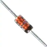
Case: DO-35 (DO-204AH)
•
•
•
•
Weight: approx. 125 mg
Cathode band color: black
Packaging codes/options:
HF-detector
Protection circuit
Small battery charger
AC/DC, DC/DC converters
TR/10K per 13" reel (52 mm tape), 50K/box
TAP/10K per ammopack (52 mm tape), 50K/box
PARTS TABLE
PART
TYPE
DIFFERENTIATION
ORDERING CODE
TYPE MARKING
CIRCUIT
CONFIGURATION
REMARKS
SD103A
VR = 40 V
SD103A-TR or SD103A-TAP
SD103A
Single
Tape and reel/ammopack
SD103B
VR = 30 V
SD103B-TR or SD103B-TAP
SD103B
Single
Tape and reel/ammopack
SD103C
VR = 20 V
SD103C-TR or SD103C-TAP
SD103C
Single
Tape and reel/ammopack
ABSOLUTE MAXIMUM RATINGS (Tamb = 25 °C, unless otherwise specified)
PARAMETER
TEST CONDITION
Peak inverse voltage
PART
SYMBOL
VALUE
UNIT
SD103A
VR
40
V
SD103B
VR
30
V
SD103C
VR
20
V
Ptot
400
mW
IFSM
15
A
SYMBOL
VALUE
UNIT
RthJA
310
K/W
Tj
125
°C
Tstg
-55 to +150
°C
Power dissipation (infinite heat sink) (1)
Peak forward surge current
tp = 300 μs square pulse
Note
(1) Valid provided that leads at a distance of 4 mm from case are kept at ambient temperature
THERMAL CHARACTERISTICS (Tamb = 25 °C, unless otherwise specified)
PARAMETER
TEST CONDITION
Thermal resistance junction to ambient air (1)
Junction temperature
Storage temperature range
Note
(1) Valid provided that leads at a distance of 4 mm from case are kept at ambient temperature
Rev. 2.0, 16-Nov-2021
Document Number: 85754
1
For technical questions within your region: DiodesAmericas@vishay.com, DiodesAsia@vishay.com, DiodesEurope@vishay.com
THIS DOCUMENT IS SUBJECT TO CHANGE WITHOUT NOTICE. THE PRODUCTS DESCRIBED HEREIN AND THIS DOCUMENT
ARE SUBJECT TO SPECIFIC DISCLAIMERS, SET FORTH AT www.vishay.com/doc?91000
�SD103A, SD103B, SD103C
www.vishay.com
Vishay Semiconductors
ELECTRICAL CHARACTERISTICS (Tamb = 25 °C, unless otherwise specified)
PARAMETER
TEST CONDITION
Reverse breakdown voltage
PART
SYMBOL
MIN.
SD103A
V(BR)
40
V
SD103B
V(BR)
30
V
SD103C
V(BR)
20
SD103A
IR
5
μA
VR = 20 V
SD103B
IR
5
μA
VR = 10 V
SD103C
IR
5
μA
VF
370
mV
600
mV
IR = 50 μA
VR = 30 V
Leakage current
IF = 20 mA
Forward voltage drop
Diode capacitance
Reverse recovery time
TYP.
MAX.
UNIT
V
IF = 200 mA
VF
VR = 0 V, f = 1 MHz
CD
50
pF
IF = IR = 50 mA to 200 mA,
recover to 0.1 IR
trr
10
ns
TYPICAL CHARACTERISTICS (Tamb = 25 °C, unless otherwise specified)
10 000
100
IR - Reverse Current (µA)
IF - Forward Current (mA)
1000
10
1
0.1
0.01
1000
100
10
0.001
1
0 100 200 300 400 500 600 700 800 900 1000
0
16767
VF - Forward Voltage (mV)
16765
Fig. 1 - Forward Current vs. Forward Voltage
20
40
60
80
100
120
140
160
Tj - Junction Temperature (°C)
Fig. 3 - Reverse Current vs. Junction Temperature
5
30
CD - Diode Capacitance (pF)
IF - Forward Current (A)
f = 1 MHz
4
3
2
1
25
20
15
10
5
0
0
0.0
16766
0.5
1.0
1.5
0
2.0
VF - Forward Voltage (V)
Fig. 2 - Forward Current vs. Forward Voltage
16768
5
10
15
20
25
30
VR - Reverse Voltage (V)
Fig. 4 - Diode Capacitance vs. Reverse Voltage
Rev. 2.0, 16-Nov-2021
Document Number: 85754
2
For technical questions within your region: DiodesAmericas@vishay.com, DiodesAsia@vishay.com, DiodesEurope@vishay.com
THIS DOCUMENT IS SUBJECT TO CHANGE WITHOUT NOTICE. THE PRODUCTS DESCRIBED HEREIN AND THIS DOCUMENT
ARE SUBJECT TO SPECIFIC DISCLAIMERS, SET FORTH AT www.vishay.com/doc?91000
�SD103A, SD103B, SD103C
www.vishay.com
Vishay Semiconductors
Itot - Typ. Non Repetitve
Forward Surge Current (A)
25
20
15
10
5
0
0.1
1.0
10.0
tP - Pulse width (ms)
16769
Fig. 5 - Typical Non-Repetitive Forward Surge Current vs.
Pulse Width
PACKAGE DIMENSIONS in millimeters (inches): DO-35 (DO-204AH)
3.9 max. [0.154]
3.1 min. [0.120]
26 min. [1.024]
1.3 [0.050]
26 min. [1.024]
1.7 [0.067]
Ø 0.4 min. [0.015]
Ø 0.6 max. [0.024]
Cathode Identification
Rev. 6 - Date: 19. December 2011
Document no.: SB-V-3906.04-031(4)
94 9366
Rev. 2.0, 16-Nov-2021
Document Number: 85754
3
For technical questions within your region: DiodesAmericas@vishay.com, DiodesAsia@vishay.com, DiodesEurope@vishay.com
THIS DOCUMENT IS SUBJECT TO CHANGE WITHOUT NOTICE. THE PRODUCTS DESCRIBED HEREIN AND THIS DOCUMENT
ARE SUBJECT TO SPECIFIC DISCLAIMERS, SET FORTH AT www.vishay.com/doc?91000
�Legal Disclaimer Notice
www.vishay.com
Vishay
Disclaimer
ALL PRODUCT, PRODUCT SPECIFICATIONS AND DATA ARE SUBJECT TO CHANGE WITHOUT NOTICE TO IMPROVE
RELIABILITY, FUNCTION OR DESIGN OR OTHERWISE.
Vishay Intertechnology, Inc., its affiliates, agents, and employees, and all persons acting on its or their behalf (collectively,
“Vishay”), disclaim any and all liability for any errors, inaccuracies or incompleteness contained in any datasheet or in any other
disclosure relating to any product.
Vishay makes no warranty, representation or guarantee regarding the suitability of the products for any particular purpose or
the continuing production of any product. To the maximum extent permitted by applicable law, Vishay disclaims (i) any and all
liability arising out of the application or use of any product, (ii) any and all liability, including without limitation special,
consequential or incidental damages, and (iii) any and all implied warranties, including warranties of fitness for particular
purpose, non-infringement and merchantability.
Statements regarding the suitability of products for certain types of applications are based on Vishay's knowledge of typical
requirements that are often placed on Vishay products in generic applications. Such statements are not binding statements
about the suitability of products for a particular application. It is the customer's responsibility to validate that a particular product
with the properties described in the product specification is suitable for use in a particular application. Parameters provided in
datasheets and / or specifications may vary in different applications and performance may vary over time. All operating
parameters, including typical parameters, must be validated for each customer application by the customer's technical experts.
Product specifications do not expand or otherwise modify Vishay's terms and conditions of purchase, including but not limited
to the warranty expressed therein.
Hyperlinks included in this datasheet may direct users to third-party websites. These links are provided as a convenience and
for informational purposes only. Inclusion of these hyperlinks does not constitute an endorsement or an approval by Vishay of
any of the products, services or opinions of the corporation, organization or individual associated with the third-party website.
Vishay disclaims any and all liability and bears no responsibility for the accuracy, legality or content of the third-party website
or for that of subsequent links.
Except as expressly indicated in writing, Vishay products are not designed for use in medical, life-saving, or life-sustaining
applications or for any other application in which the failure of the Vishay product could result in personal injury or death.
Customers using or selling Vishay products not expressly indicated for use in such applications do so at their own risk. Please
contact authorized Vishay personnel to obtain written terms and conditions regarding products designed for such applications.
No license, express or implied, by estoppel or otherwise, to any intellectual property rights is granted by this document or by
any conduct of Vishay. Product names and markings noted herein may be trademarks of their respective owners.
© 2022 VISHAY INTERTECHNOLOGY, INC. ALL RIGHTS RESERVED
Revision: 01-Jan-2022
1
Document Number: 91000
�


 工商网监
湘ICP备2023018690号
工商网监
湘ICP备2023018690号
