Si1023X
Vishay Siliconix
Dual P-Channel 20 V (D-S) MOSFET
FEATURES
PRODUCT SUMMARY
VDS (V)
- 20
RDS(on) ()
ID (mA)
1.2 at VGS = - 4.5 V
- 350
1.6 at VGS = - 2.5 V
- 300
2.7 at VGS = - 1.8 V
- 150
• Halogen-free According to IEC 61249-2-21
Definition
• TrenchFET® Power MOSFET: 1.8 V Rated
• Very Small Footprint
• High-Side Switching
• Low On-Resistance: 1.2
• Low Threshold: 0.8 V (typ.)
• Fast Switching Speed: 14 ns
• 1.8 V Operation
• Gate-Source ESD Protected: 2000 V
• Compliant to RoHS Directive 2002/95/EC
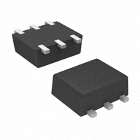
SOT-563
SC-89
BENEFITS
S1
1
6
D1
G1
2
5
G2
D2
3
4
S2
Marking Code: B
•
•
•
•
•
Ease in Driving Switches
Low Offset (Error) Voltage
Low-Voltage Operation
High-Speed Circuits
Low Battery Voltage Operation
APPLICATIONS
Top View
Ordering Information: Si1023X-T1-GE3 (Lead (Pb)-free and Halogen-free)
• Drivers: Relays, Solenoids, Lamps, Hammers, Displays,
Memories
• Battery Operated Systems
• Power Supply Converter Circuits
• Load/Power Switching Cell Phones, Pagers
ABSOLUTE MAXIMUM RATINGS (TA = 25 °C, unless otherwise noted)
Parameter
Symbol
5s
Steady State
Drain-Source Voltage
VDS
- 20
Gate-Source Voltage
VGS
±6
Continuous Drain Current (TJ = 150 °C)a
Pulsed Drain
TA = 25 °C
TA = 85 °C
Currentb
Operating Junction and Storage Temperature Range
Gate-Source ESD Rating (HBM, Method 3015)
- 390
IS
TA = 25 °C
TA = 85 °C
PD
V
- 370
- 280
IDM
Continuous Source Current (Diode Conduction)a
Maximum Power Dissipationa
ID
Unit
- 265
- 650
- 450
- 380
280
250
145
130
mA
mW
TJ, Tstg
- 55 to 150
°C
ESD
2000
V
Notes:
a. Surface mounted on FR4 board.
b. Pulse width limited by maximum junction temperature.
Document Number: 71169
S10-2432-Rev. C, 25-Oct-10
www.vishay.com
1
�Si1023X
Vishay Siliconix
SPECIFICATIONS (TJ = 25 °C, unless otherwise noted)
Parameter
Symbol
Test Conditions
Min.
- 0.45
Typ.
Max.
Unit
µA
Static
VGS(th)
VDS = VGS, ID = - 250 µA
Gate-Body Leakage
IGSS
VDS = 0 V, VGS = ± 4.5 V
±1
±2
Zero Gate Voltage Drain Current
IDSS
VDS = - 16 V, VGS = 0 V
- 0.3
- 100
nA
-5
µA
On-State Drain Currenta
ID(on)
VDS = - 5 V, VGS = - 4.5 V
VGS = - 4.5 V, ID = - 350 mA
0.8
1.2
RDS(on)
VGS = - 2.5 V, ID = - 300 mA
1.2
1.6
VGS = - 1.8 V, ID = - 150 mA
1.8
2.7
gfs
VDS = - 10 V, ID = - 250 mA
0.4
VSD
IS = - 150 mA, VGS = 0 V
- 0.8
Gate Threshold Voltage
Drain-Source On-State
Resistancea
Forward Transconductancea
Diode Forward Voltage
a
V
VDS = - 16 V, VGS = 0 V, TJ = 85 °C
- 700
mA
S
- 1.2
V
Dynamicb
Total Gate Charge
Qg
Gate-Source Charge
Qgs
Gate-Drain Charge
Qgd
Turn-On Time
td(on)
Turn-Off Time
td(off)
1500
VDS = - 10 V, VGS = - 4.5 V, ID = - 250 mA
pC
150
450
VDD = -10 V, RL = 47
ID - 200 mA, VGEN = - 4.5 V, Rg = 10
14
ns
46
Notes:
a. Pulse test; pulse width 300 µs, duty cycle 2 %.
b. Guaranteed by design, not subject to production testing.
Stresses beyond those listed under “Absolute Maximum Ratings” may cause permanent damage to the device. These are stress ratings only, and functional operation
of the device at these or any other conditions beyond those indicated in the operational sections of the specifications is not implied. Exposure to absolute maximum
rating conditions for extended periods may affect device reliability.
TYPICAL CHARACTERISTICS (TA = 25 °C, unless otherwise noted)
1.0
1000
VGS = 5 V thru 3 V
TJ = - 55 °C
2.5 V
0.6
2V
0.4
1.8 V
0.2
0.0
0.0
600
125 °C
400
200
0.5
1.0
1.5
2.0
VDS - Drain-to-Source Voltage (V)
Output Characteristics
www.vishay.com
2
25 °C
800
I D - Drain Current (mA)
I D - Drain Current (A)
0.8
2.5
3.0
0
0.0
0.5
1.0
1.5
2.0
2.5
3.0
VGS - Gate-to-Source Voltage (V)
Transfer Characteristics
Document Number: 71169
S10-2432-Rev. C, 25-Oct-10
�Si1023X
Vishay Siliconix
TYPICAL CHARACTERISTICS (TA = 25 °C, unless otherwise noted)
120
VGS = 1.8 V
2.4
VGS = 2.5 V
1.6
VGS = 4.5 V
Ciss
80
60
40
Coss
0.8
20
Crss
0.0
0
0
200
400
600
800
1000
0
4
8
12
16
I D - Drain Current (mA)
VDS - Drain-to-Source Voltage (V)
On-Resistance vs. Drain Current
Capacitance
20
1.6
5
VDS = 10 V
ID = 250 mA
1.4
3
2
VGS = 4.5 V
ID = 350 mA
1.2
VGS = 1.8 V
ID = 150 mA
1.0
0.8
1
0
0.0
(Normalized)
4
R DS(on) - On-Resistance
VGS - Gate-to-Source Voltage (V)
VGS = 0 V
f = 1 MHz
100
3.2
C - Capacitance (pF)
R DS(on) - On-Resistance (Ω)
4.0
0.2
0.4
0.6
0.8
1.0
1.2
1.4
0.6
- 50
1.6
- 25
0
25
50
75
100
Q g - Total Gate Charge (nC)
TJ - Junction Temperature (°C)
Gate Charge
On-Resistance vs. Junction Temperature
1000
125
5
R DS(on) - On-Resistance (Ω)
I S - Source Current (mA)
TJ = 125 °C
100
TJ = 25 °C
TJ = - 55 °C
10
1
0.0
4
3
ID = 350 mA
2
ID = 200 mA
1
0
0.2
0.4
0.6
0.8
1.0
1.2
1.4
0
1
2
3
4
5
VSD - Sour ce-to-Drain Voltage (V)
VGS - Gate-to-Source Voltage (V)
Source-Drain Diode Forward Voltage
On-Resistance vs. Gate-to-Source Voltage
Document Number: 71169
S10-2432-Rev. C, 25-Oct-10
6
www.vishay.com
3
�Si1023X
Vishay Siliconix
TYPICAL CHARACTERISTICS (TA = 25 °C, unless otherwise noted)
0.3
3.0
2.5
ID = 0.25 mA
0.1
2.0
IGSS - (µA)
VGS(th) Variance (V)
0.2
0.0
VGS = 4.5 V
1.5
- 0.1
1.0
- 0.2
0.5
- 0.3
- 50
- 25
0
25
50
75
100
0.0
- 50
125
- 25
0
TJ - Temperature (°C)
50
75
100
125
TJ - Temperature (°C)
Threshold Voltage Variance vs. Temperature
BVGSS - Gate-to-Source Breakdown Voltage (V)
25
IGSS vs. Temperature
7
6
5
4
3
2
1
0
- 50
- 25
0
25
50
75
100
125
TJ - Temperature (°C)
BVGSS vs. Temperature
Normalized Effective Transient
Thermal Impedance
2
1
Duty Cycle = 0.5
0.2
Notes:
0.1
PDM
0.1
0.05
t1
t2
1. Duty Cycle, D =
t1
t2
2. Per Unit Base = RthJA = 500 °C/W
0.02
3. TJM - TA = PDMZthJA(t)
Single Pulse
4. Surface Mounted
0.01
10 -4
10 -3
10 -2
10 -1
1
Square Wave Pulse Duration (s)
10
100
600
Normalized Thermal Transient Impedance, Junction-to-Ambient
Vishay Siliconix maintains worldwide manufacturing capability. Products may be manufactured at one of several qualified locations. Reliability data for Silicon
Technology and Package Reliability represent a composite of all qualified locations. For related documents such as package/tape drawings, part marking, and
reliability data, see www.vishay.com/ppg?71169.
www.vishay.com
4
Document Number: 71169
S10-2432-Rev. C, 25-Oct-10
�Package Information
www.vishay.com
Vishay Siliconix
SC-89 6-Leads (SOT-563F)
E1/2
2
3
aaa
D
e1
4
C
2x
4
A
B
D
6
5
4
SECTION B-B
C
E/2
2
E
E1
3
6
2x
DETAIL “A”
aaa
C
1
5
2
2x
3
bbb
C
e
B
6x b
4
ddd
M
C
A–B D
L1
A1
L
A
A1
SEE DETAIL “A”
Notes
1. Dimensions in millimeters.
2. Dimension D does not include mold flash, protrusions or gate
burrs. Mold flush, protrusions or gate burrs shall not exceed
0.15 mm per dimension E1 does not include interlead flash
or protrusion, interlead flash or protrusion shall not exceed
0.15 mm per side.
3. Dimensions D and E1 are determined at the outmost extremes
of the plastic body exclusive of mold flash, the bar burrs, gate
burrs and interlead flash, but including any mismatch between
the top and the bottom of the plastic body.
4. Datums A, B and D to be determined 0.10 mm from the lead tip.
5. Terminal numbers are shown for reference only.
6. These dimensions apply to the flat section of the lead between
0.08 mm and 0.15 mm from the lead tip.
Revision: 11-Aug-14
DIM.
MILLIMETERS
MIN.
NOM.
A
0.56
0.58
MAX.
0.60
A1
0
0.02
0.10
b
0.15
0.22
0.30
0.18
c
0.10
0.14
D
1.50
1.60
1.70
E
1.50
1.60
1.70
1.25
E1
1.15
1.20
e
0.45
0.50
0.55
e1
0.95
1.00
1.05
L
0.25
0.35
0.50
L1
0.10
0.20
0.30
C14-0439-Rev. C, 11-Aug-14
DWG: 5880
Document Number: 71612
1
For technical questions, contact: analogswitchtechsupport@vishay.com
THIS DOCUMENT IS SUBJECT TO CHANGE WITHOUT NOTICE. THE PRODUCTS DESCRIBED HEREIN AND THIS DOCUMENT
ARE SUBJECT TO SPECIFIC DISCLAIMERS, SET FORTH AT www.vishay.com/doc?91000
�Application Note 826
Vishay Siliconix
RECOMMENDED MINIMUM PADS FOR SC-89: 6-Lead
0.051
0.012
0.020
(0.300)
(0.500)
0.019
(0.478)
0.031
(0.798)
0.069
(1.753)
(1.300)
0.051
(0.201)
Recommended Minimum Pads
Dimensions in Inches/(mm)
Return to Index
Return to Index
APPLICATION NOTE
Document Number: 72605
Revision: 21-Jan-08
www.vishay.com
21
�Legal Disclaimer Notice
www.vishay.com
Vishay
Disclaimer
ALL PRODUCT, PRODUCT SPECIFICATIONS AND DATA ARE SUBJECT TO CHANGE WITHOUT NOTICE TO IMPROVE
RELIABILITY, FUNCTION OR DESIGN OR OTHERWISE.
Vishay Intertechnology, Inc., its affiliates, agents, and employees, and all persons acting on its or their behalf (collectively,
“Vishay”), disclaim any and all liability for any errors, inaccuracies or incompleteness contained in any datasheet or in any other
disclosure relating to any product.
Vishay makes no warranty, representation or guarantee regarding the suitability of the products for any particular purpose or
the continuing production of any product. To the maximum extent permitted by applicable law, Vishay disclaims (i) any and all
liability arising out of the application or use of any product, (ii) any and all liability, including without limitation special,
consequential or incidental damages, and (iii) any and all implied warranties, including warranties of fitness for particular
purpose, non-infringement and merchantability.
Statements regarding the suitability of products for certain types of applications are based on Vishay's knowledge of typical
requirements that are often placed on Vishay products in generic applications. Such statements are not binding statements
about the suitability of products for a particular application. It is the customer's responsibility to validate that a particular product
with the properties described in the product specification is suitable for use in a particular application. Parameters provided in
datasheets and / or specifications may vary in different applications and performance may vary over time. All operating
parameters, including typical parameters, must be validated for each customer application by the customer's technical experts.
Product specifications do not expand or otherwise modify Vishay's terms and conditions of purchase, including but not limited
to the warranty expressed therein.
Hyperlinks included in this datasheet may direct users to third-party websites. These links are provided as a convenience and
for informational purposes only. Inclusion of these hyperlinks does not constitute an endorsement or an approval by Vishay of
any of the products, services or opinions of the corporation, organization or individual associated with the third-party website.
Vishay disclaims any and all liability and bears no responsibility for the accuracy, legality or content of the third-party website
or for that of subsequent links.
Except as expressly indicated in writing, Vishay products are not designed for use in medical, life-saving, or life-sustaining
applications or for any other application in which the failure of the Vishay product could result in personal injury or death.
Customers using or selling Vishay products not expressly indicated for use in such applications do so at their own risk. Please
contact authorized Vishay personnel to obtain written terms and conditions regarding products designed for such applications.
No license, express or implied, by estoppel or otherwise, to any intellectual property rights is granted by this document or by
any conduct of Vishay. Product names and markings noted herein may be trademarks of their respective owners.
© 2022 VISHAY INTERTECHNOLOGY, INC. ALL RIGHTS RESERVED
Revision: 01-Jan-2022
1
Document Number: 91000
�


 工商网监
湘ICP备2023018690号
工商网监
湘ICP备2023018690号
