Si1539DDL
www.vishay.com
Vishay Siliconix
N- and P-Channel 30 V (D-S) MOSFET
FEATURES
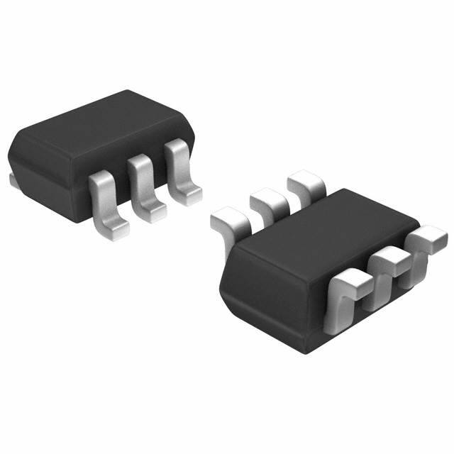
SOT-363
SC-70 Dual (6 leads)
D1
6
• TrenchFET® power MOSFET
S2
4
G2
5
• 100 % Rg tested
• Material categorization:
for definitions of compliance please see
www.vishay.com/doc?99912
1
S1
Top View
2
G1
APPLICATIONS
3
D2
• DC/DC converter
• Load switch
D1
Marking code: RI
S2
PRODUCT SUMMARY
N-CHANNEL
P-CHANNEL
30
-30
VDS (V)
RDS(on) (Ω) at VGS = ± 10 V
0.388
1.070
RDS(on) (Ω) at VGS = ± 4.5 V
0.525
2.590
Qg typ. (nC)
0.55
0.8
ID (A) a
0.7
-0.46
Configuration
G2
G1
Dual
S1
D2
N-Channel MOSFET
P-Channel MOSFET
ORDERING INFORMATION
Package
SOT-363
Lead (Pb)-free and halogen-free
Si1539DDL-T1-GE3
ABSOLUTE MAXIMUM RATINGS (TA = 25 °C, unless otherwise noted)
PARAMETER
SYMBOL
N-CHANNEL
P-CHANNEL
Drain-source voltage
VDS
30
-30
Gate-source voltage
VGS
± 20
± 20
Continuous drain current (TJ = 150 °C)
Source-drain current diode current
TC = 25 °C
0.7
-0.46
TC = 70 °C
0.6
-0.36
ID
0.7 b, c
-0.42 b, c
0.5 b, c
-0.33 b, c
TC = 25 °C
0.3
-0.3
0.2 b, c
-0.2 b, c
TA = 25 °C
Pulsed drain current (t = 100 μs)
IS
IDM
TC = 25 °C
TC = 70 °C
Maximum power dissipation
V
TA = 70 °C
TA = 25 °C
TA = 25 °C
PD
-1
0.34
0.34
0.22
0.22
0.29 b, c
0.29 b, c
0.18 b, c
TA = 70 °C
Operating junction and storage temperature range
2
TJ, Tstg
UNIT
A
W
0.18 b, c
-55 to +150
°C
THERMAL RESISTANCE RATINGS
PARAMETER
Maximum junction-to-ambient
SYMBOL
b, d
t ≤ 10 s
RthJA
N-CHANNEL
MAX.
TYP.
MAX.
365
438
365
438
370
308
370
308
Maximum junction-to-foot (drain)
Steady state
RthJF
Notes
a. Based on TC = 25 °C
b. Surface mounted on 1" x 1" FR4 board
c. t = 10 s
d. Maximum under steady state conditions is 486 °C/W (N-Channel) and 486 °C/W (P-Channel)
S17-1009-Rev. B, 03-Jul-17
P-CHANNEL
TYP.
UNIT
°C/W
Document Number: 62999
1
For technical questions, contact: pmostechsupport@vishay.com
THIS DOCUMENT IS SUBJECT TO CHANGE WITHOUT NOTICE. THE PRODUCTS DESCRIBED HEREIN AND THIS DOCUMENT
ARE SUBJECT TO SPECIFIC DISCLAIMERS, SET FORTH AT www.vishay.com/doc?91000
�Si1539DDL
www.vishay.com
Vishay Siliconix
SPECIFICATIONS (TJ = 25 °C, unless otherwise noted)
PARAMETER
SYMBOL
TEST CONDITIONS
MIN.
TYP. a
MAX.
UNIT
Static
Drain-source breakdown voltage
VDS temperature coefficient
VDS
ΔVDS/TJ
VGS(th) temperature coefficient
ΔVGS(th)/TJ
Gate-source threshold voltage
VGS(th)
Gate-body leakage
IGSS
VGS = 0 V, ID = 250 μA
N-Ch
30
-
-
VGS = 0 V, ID = -250 μA
P-Ch
-30
-
-
ID = 250 μA
N-Ch
-
30
-
ID = -250 μA
P-Ch
-
-25
-
ID = 250 μA
N-Ch
-
-3.6
-
ID = -250 μA
P-Ch
-
3.1
-
VDS = VGS, ID = 250 μA
N-Ch
1.2
-
2.5
VDS = VGS, ID = -250 μA
P-Ch
-1.5
-
-3
VDS = 0 V, VGS = ± 20 V
VDS = 30 V, VGS = 0 V
Zero gate voltage drain current
On-state drain current b
Drain-source on-state resistance b
IDSS
ID(on)
RDS(on)
-
± 100
-
-
± 100
N-Ch
-
-
1
VDS = -30 V, VGS = 0 V
P-Ch
-
-
-1
N-Ch
-
-
10
VDS = -30 V, VGS = 0 V, TJ = 55 °C
P-Ch
-
-
-10
VDS = 5 V, VGS = 10 V
N-Ch
2
-
-
VDS = -5 V, VGS = -10 V
P-Ch
-1
-
-
VGS = 10 V, ID = 0.6 A
N-Ch
-
0.323
0.388
VGS = -10 V, ID = -0.4 A
P-Ch
-
0.890
1.070
VGS = 4.5 V, ID = 0.1A
N-Ch
-
0.437
0.525
VGS = -5 V, ID = -0.1 A
gfs
-
P-Ch
VDS = 30 V, VGS = 0 V, TJ = 55 °C
VGS = -4.35 V, ID = -0.1 A
Forward transconductance b
N-Ch
P-Ch
-
1.850
2.590
-
2.800
-
VDS = 15 V, ID = 0.6 A
N-Ch
-
1.2
-
VDS = -15 V, ID = -0.4 A
P-Ch
-
0.6
-
V
mV/°C
V
nA
μA
A
Ω
S
Dynamic a
Input capacitance
Ciss
N-Channel
VDS = 15 V, VGS = 0 V, f = 1 MHz
Output capacitance
Coss
P-Channel
VDS = -15 V, VGS = 0 V, f = 1 MHz
Reverse transfer capacitance
Total gate charge
Gate-source charge
Crss
Qg
Qgd
Gate resistance
Rg
S17-1009-Rev. B, 03-Jul-17
-
28
-
P-Ch
-
21
-
N-Ch
-
10
-
P-Ch
-
10
-
N-Ch
-
5
-
P-Ch
-
6
-
VDS = 15 V, VGS = 10 V, ID = 0.6 A
N-Ch
-
1
1.5
VDS = -15 V, VGS = -10 V, ID = -0.4 A
P-Ch
-
1.5
3
N-Ch
-
0.55
1.1
N-Channel
VDS = 15 V, VGS = 4.5 V ID = 0.6 A
P-Ch
-
0.8
1.2
N-Ch
-
0.2
-
P-Channel
VDS = -15 V, VGS = -4.5 V, ID = -0.4 A
P-Ch
-
0.4
-
N-Ch
-
0.2
-
P-Ch
-
0.35
-
N-Ch
0.7
3.7
7.4
P-Ch
0.3
15
30
Qgs
Gate-drain charge
N-Ch
f = 1 MHz
pF
nC
Ω
Document Number: 62999
2
For technical questions, contact: pmostechsupport@vishay.com
THIS DOCUMENT IS SUBJECT TO CHANGE WITHOUT NOTICE. THE PRODUCTS DESCRIBED HEREIN AND THIS DOCUMENT
ARE SUBJECT TO SPECIFIC DISCLAIMERS, SET FORTH AT www.vishay.com/doc?91000
�Si1539DDL
www.vishay.com
Vishay Siliconix
SPECIFICATIONS (TJ = 25 °C, unless otherwise noted)
PARAMETER
Dynamic
SYMBOL
MIN.
TYP. a
MAX.
N-Ch
-
2
4
P-Ch
-
4
8
N-Ch
-
14
21
P-Ch
-
18
30
N-Ch
-
11
20
P-Ch
-
8
16
N-Ch
-
9
18
TEST CONDITIONS
UNIT
a
Turn-on delay time
td(on)
Rise time
Turn-off delay time
tr
td(off)
Fall time
Turn-on delay time
P-Channel
VDD = -15 V, RL = 38 Ω
ID ≅ -0.4 A, VGEN = -10 V, Rg = 1 Ω
tf
td(on)
Rise time
Turn-off delay time
N-Channel
VDD = 15 V, RL = 30 Ω
ID ≅ 0.5 A, VGEN = 10 V, Rg = 1 Ω
tr
td(off)
Fall Time
N-Channel
VDD = 15 V, RL = 30 Ω
ID ≅ 0.5 A, VGEN = 4.5 V, Rg = 1 Ω
P-Channel
VDD = -15 V, RL = 50 Ω
ID ≅ -0.3 A, VGEN = -4.5 V, Rg = 1 Ω
tf
P-Ch
-
18
30
N-Ch
-
26
39
P-Ch
-
22
33
N-Ch
-
25
38
P-Ch
-
28
42
N-Ch
-
14
21
P-Ch
-
4
8
N-Ch
-
15
23
P-Ch
-
18
30
N-Ch
-
-
0.3
ns
Drain-Source Body Diode Characteristics
Continuous source-drain diode current
Pulse diode forward current
(t = 100 μs)
Body diode voltage
IS
ISM
VSD
Body diode reverse recovery time
trr
Body diode reverse recovery charge
Qrr
Reverse recovery fall time
ta
Reverse recovery rise time
TC = 25 °C
P-Ch
-
-
-0.3
N-Ch
-
-
2
P-Ch
-
-
-1
IS = 0.5 A
N-Ch
-
0.8
1.2
IS = -0.4 A
P-Ch
-
-0.8
-1.2
N-Ch
-
10
20
P-Ch
-
13
20
N-Channel
IF = 0.5 A, di/dt = 100 A/μs, TJ = 25 °C
N-Ch
-
3
6
P-Ch
-
8
16
P-Channel
IF = -0.5 A, di/dt = -100 A/μs, TJ = 25 °C
N-Ch
-
6
-
tb
P-Ch
-
7
-
N-Ch
-
4
-
P-Ch
-
6
-
A
V
ns
nC
ns
Notes
a. Guaranteed by design, not subject to production testing
b. Pulse test; pulse width ≤ 300 μs, duty cycle ≤ 2 %
Stresses beyond those listed under “Absolute Maximum Ratings” may cause permanent damage to the device. These are stress ratings only, and functional operation
of the device at these or any other conditions beyond those indicated in the operational sections of the specifications is not implied. Exposure to absolute maximum
rating conditions for extended periods may affect device reliability.
S17-1009-Rev. B, 03-Jul-17
Document Number: 62999
3
For technical questions, contact: pmostechsupport@vishay.com
THIS DOCUMENT IS SUBJECT TO CHANGE WITHOUT NOTICE. THE PRODUCTS DESCRIBED HEREIN AND THIS DOCUMENT
ARE SUBJECT TO SPECIFIC DISCLAIMERS, SET FORTH AT www.vishay.com/doc?91000
�Si1539DDL
www.vishay.com
Vishay Siliconix
N-CHANNEL TYPICAL CHARACTERISTICS (25 °C, unless otherwise noted)
2
0.5
VGS = 10 V thru 5 V
VGS = 4 V
0.4
ID - Drain Current (A)
ID - Drain Current (A)
1.5
1
0.3
TC = 25 °C
0.2
0.5
0.1
VGS = 3 V
TC = 125 °C
TC = - 55 °C
0
0
0.5
1
1.5
2
0
1
2
3
4
VDS - Drain-to-Source Voltage (V)
VGS - Gate-to-Source Voltage (V)
Output Characteristics
Transfer Characteristics
0.80
40
0.60
30
C - Capacitance (pF)
RDS(on) - On-Resistance (Ω)
0
VGS = 4.5 V
0.40
VGS = 10 V
0.20
Ciss
20
Coss
10
Crss
0.00
0
0
0.5
1
1.5
2
0
12
18
24
ID - Drain Current (A)
VDS - Drain-to-Source Voltage (V)
On-Resistance vs. Drain Current and Gate Voltage
Capacitance
10
30
1.8
8
RDS(on) - On-Resistance (Normalized)
ID = 0.6 A
VGS - Gate-to-Source Voltage (V)
6
VDS = 7.5 V
6
VDS = 15 V
4
VDS = 24 V
2
0
0
0.3
0.6
0.9
Qg - Total Gate Charge (nC)
Gate Charge
S17-1009-Rev. B, 03-Jul-17
1.2
VGS = 10 V
ID = 0.6 A
1.5
1.2
0.9
0.6
- 50
VGS = 4.5 V
- 25
0
25
50
75
100
125
150
TJ - Junction Temperature (°C)
On-Resistance vs. Junction Temperature
Document Number: 62999
4
For technical questions, contact: pmostechsupport@vishay.com
THIS DOCUMENT IS SUBJECT TO CHANGE WITHOUT NOTICE. THE PRODUCTS DESCRIBED HEREIN AND THIS DOCUMENT
ARE SUBJECT TO SPECIFIC DISCLAIMERS, SET FORTH AT www.vishay.com/doc?91000
�Si1539DDL
www.vishay.com
Vishay Siliconix
N-CHANNEL TYPICAL CHARACTERISTICS (25 °C, unless otherwise noted)
0.8
10
1
TJ = 25 °C
0.1
0.0
VGS(th) (V)
RDS(on) - On-Resistance (Ω)
TJ = 150 °C
0.6
TJ = 25 °C
0.2
0
0.3
0.6
0.9
1.2
1.5
2
4
6
8
10
VSD - Source-to-Drain Voltage (V)
VGS - Gate-to-Source Voltage (V)
Source-Drain Diode Forward Voltage
On-Resistance vs. Gate-to-Source Voltage
2
6.4
1.8
4.8
ID = 250 μA
1.6
1.4
1.2
- 50
TJ = 125 °C
0.4
Power (W)
IS - Source Current (A)
ID = 0.6 A
3.2
1.6
- 25
0
25
50
75
100
125
0
0.001
150
0.01
0.1
1
TJ - Temperature (°C)
Time (s)
Threshold Voltage
Single Pulse Power, Junction-to-Ambient
10
10
Limited by IDM
ID - Drain Current (A)
Limited by RDS(on)*
BVDSS Limited
1
100 μs
1 ms
0.1
10 ms
100 ms
TA = 25 °C
Single Pulse
0.01
0.1
1s
10 s, DC
100
1
10
VDS - Drain-to-Source Voltage (V)
* VGS > minimum VGS at which RDS(on) is specified
Safe Operating Area, Junction-to-Ambient
S17-1009-Rev. B, 03-Jul-17
Document Number: 62999
5
For technical questions, contact: pmostechsupport@vishay.com
THIS DOCUMENT IS SUBJECT TO CHANGE WITHOUT NOTICE. THE PRODUCTS DESCRIBED HEREIN AND THIS DOCUMENT
ARE SUBJECT TO SPECIFIC DISCLAIMERS, SET FORTH AT www.vishay.com/doc?91000
�Si1539DDL
www.vishay.com
Vishay Siliconix
N-CHANNEL TYPICAL CHARACTERISTICS (25 °C, unless otherwise noted)
0.8
ID - Drain Current (A)
0.6
0.4
0.2
0
0
25
50
75
100
125
150
0
25
TC - Case Temperature (°C)
Current Derating a
0.45
0.32
0.36
0.27
Power (W)
Power (W)
0.24
0.18
0.16
0.08
0.09
0
0
0
25
50
75
100
125
TC - Case Temperature (°C)
Power Derating, Junction-to-Foot
150
50
75
100
125
150
TA - Ambient Temperature (°C)
Power Derating, Junction-to-Ambient
Note
a. The power dissipation PD is based on TJ max. = 150 °C, using junction-to-case thermal resistance, and is more useful in settling the upper
dissipation limit for cases where additional heatsinking is used. It is used to determine the current rating, when this rating falls below the
package limit
S17-1009-Rev. B, 03-Jul-17
Document Number: 62999
6
For technical questions, contact: pmostechsupport@vishay.com
THIS DOCUMENT IS SUBJECT TO CHANGE WITHOUT NOTICE. THE PRODUCTS DESCRIBED HEREIN AND THIS DOCUMENT
ARE SUBJECT TO SPECIFIC DISCLAIMERS, SET FORTH AT www.vishay.com/doc?91000
�Si1539DDL
www.vishay.com
Vishay Siliconix
N-CHANNEL TYPICAL CHARACTERISTICS (25 °C, unless otherwise noted)
Normalized Effective Transient
Thermal Impedance
1
Duty Cycle = 0.5
0.2
Notes:
0.1
0.1
PDM
0.05
t1
t2
1. Duty Cycle, D =
0.02
t1
t2
2. Per Unit Base = R thJA = 486 °C/W
3. T JM - TA = PDMZthJA(t)
Single Pulse
4. Surface Mounted
0.01
0.0001
0.001
0.01
0.1
1
10
100
Square Wave Pulse Duration (s)
Normalized Thermal Transient Impedance, Junction-to-Ambient
Normalized Effective Transient
Thermal Impedance
1
Duty Cycle = 0.5
0.2
0.1
0.1
0.05
0.02
Single Pulse
0.01
0.0001
0.001
0.01
0.1
1
10
Square Wave Pulse Duration (s)
Normalized Thermal Transient Impedance, Junction-to-Foot
S17-1009-Rev. B, 03-Jul-17
Document Number: 62999
7
For technical questions, contact: pmostechsupport@vishay.com
THIS DOCUMENT IS SUBJECT TO CHANGE WITHOUT NOTICE. THE PRODUCTS DESCRIBED HEREIN AND THIS DOCUMENT
ARE SUBJECT TO SPECIFIC DISCLAIMERS, SET FORTH AT www.vishay.com/doc?91000
�Si1539DDL
www.vishay.com
Vishay Siliconix
P-CHANNEL TYPICAL CHARACTERISTICS (25 °C, unless otherwise noted)
0.1
1
VGS = 10V thru 7V
VGS = 6 V
0.08
0.5
ID - Drain Current (A)
ID - Drain Current (A)
0.75
VGS = 5 V
TC = 125 °C
0.06
0.04
TC = 25 °C
0.25
VGS = 4 V
0.02
TC = - 55 °C
0
0
0.5
1
1.5
0
2
0
0.6
VDS - Drain-to-Source Voltage (V)
4.6
36
3.95
30
VGS = 4.35 V
3.3
2.65
C - Capacitance (pF)
RDS(on) - On-Resistance (Ω)
3.6
Transfer Characteristics
Output Characteristics
VGS = 4.5 V
2
1.35
24
Ciss
18
12
Coss
VGS = 10 V
Crss
6
0.7
0.05
0
0
0.1
0.2
0.3
0.4
0.5
ID - Drain Current (A)
0
12
18
24
VDS - Drain-to-Source Voltage (V)
On-Resistance vs. Drain Current and Gate Voltage
Capacitance
6
30
1.6
10
VDS = 8 V
VGS = 10 V,, 0.4 A
RDS(on) - On-Resistance (Normalized)
ID = 0.4 A
VGS - Gate-to-Source Voltage (V)
1.2
1.8
2.4
3
VGS - Gate-to-Source Voltage (V)
8
VDS = 15 V
6
4
VDS = 24 V
2
0
0
0.3
0.6
0.9
1.2
1.4
1.2
VGS = 5 V, 0.1 A
1
0.8
0.6
- 50
- 25
0
25
50
75
100
125
150
Qg - Total Gate Charge (nC)
TJ - Junction Temperature (°C)
Gate Charge
On-Resistance vs. Junction Temperature
S17-1009-Rev. B, 03-Jul-17
Document Number: 62999
8
For technical questions, contact: pmostechsupport@vishay.com
THIS DOCUMENT IS SUBJECT TO CHANGE WITHOUT NOTICE. THE PRODUCTS DESCRIBED HEREIN AND THIS DOCUMENT
ARE SUBJECT TO SPECIFIC DISCLAIMERS, SET FORTH AT www.vishay.com/doc?91000
�Si1539DDL
www.vishay.com
Vishay Siliconix
P-CHANNEL TYPICAL CHARACTERISTICS (25 °C, unless otherwise noted)
4
10
RDS(on) - On-Resistance (Ω)
IS - Source Current (A)
ID = 0.4 A
TJ = 150 °C
1
TJ = 25 °C
3
2
TJ = 125 °C
1
TJ = 25 °C
0
0.1
0.0
0.4
0.8
1.2
1.6
4
6
8
10
VSD - Source-to-Drain Voltage (V)
VGS - Gate-to-Source Voltage (V)
Source-Drain Diode Forward Voltage
On-Resistance vs. Gate-to-Source Voltage
6.4
2.55
ID = 250 μA
4.8
Power (W)
VGS(th) (V)
2.35
2.15
1.6
1.95
1.75
- 50
3.2
- 25
0
25
50
75
100
125
0
0.001
150
0.01
0.1
1
TJ - Temperature (°C)
Time (s)
Threshold Voltage
Single Pulse Power, Junction-to-Ambient
10
10
Limited by IDM
ID - Drain Current (A)
1
100 μs
1 ms
Limited by RDS(on)*
0.1
10 ms
100 ms
1s
DC,10 s
0.01
TA = 25 °C
BVDSS Limited
0.001
0.1
1
10
100
VDS - Drain-to-Source Voltage (V)
* VGS > minimum VGS at which RDS(on) is specified
Safe Operating Area, Junction-to-Ambient
S17-1009-Rev. B, 03-Jul-17
Document Number: 62999
9
For technical questions, contact: pmostechsupport@vishay.com
THIS DOCUMENT IS SUBJECT TO CHANGE WITHOUT NOTICE. THE PRODUCTS DESCRIBED HEREIN AND THIS DOCUMENT
ARE SUBJECT TO SPECIFIC DISCLAIMERS, SET FORTH AT www.vishay.com/doc?91000
�Si1539DDL
www.vishay.com
Vishay Siliconix
P-CHANNEL TYPICAL CHARACTERISTICS (25 °C, unless otherwise noted)
0.55
ID - Drain Current (A)
0.44
0.33
0.22
0.11
0
0
25
50
75
100
125
150
0
25
TC - Case Temperature (°C)
Current Derating a
0.32
0.45
0.36
0.27
Power (W)
Power (W)
0.24
0.18
0.16
0.08
0.09
0.00
0
0
25
50
75
100
125
150
50
75
100
125
TC - Case Temperature (°C)
TA - Ambient Temperature (°C)
Power Derating, Junction-to-Foot
Power Derating, Junction-to-Ambient
150
Note
a. The power dissipation PD is based on TJ max. = 150 °C, using junction-to-case thermal resistance, and is more useful in
settling the upper dissipation limit for cases where additional heatsinking is used. It is used to determine the current rating,
when this rating falls below the package limit
S17-1009-Rev. B, 03-Jul-17
Document Number: 62999
10
For technical questions, contact: pmostechsupport@vishay.com
THIS DOCUMENT IS SUBJECT TO CHANGE WITHOUT NOTICE. THE PRODUCTS DESCRIBED HEREIN AND THIS DOCUMENT
ARE SUBJECT TO SPECIFIC DISCLAIMERS, SET FORTH AT www.vishay.com/doc?91000
�Si1539DDL
www.vishay.com
Vishay Siliconix
P-CHANNEL TYPICAL CHARACTERISTICS (25 °C, unless otherwise noted)
Normalized Effective Transient
Thermal Impedance
1
Duty Cycle = 0.5
0.2
Notes:
0.1
0.1
PDM
0.05
t1
t2
1. Duty Cycle, D =
0.02
t1
t2
2. Per Unit Base = R thJA = 486 °C/W
3. T JM - TA = PDMZthJA(t)
Single Pulse
4. Surface Mounted
0.01
0.0001
0.001
0.01
0.1
1
10
100
Square Wave Pulse Duration (s)
Normalized Thermal Transient Impedance, Junction-to-Ambient
Normalized Effective Transient
Thermal Impedance
1
Duty Cycle = 0.5
0.2
0.1
0.1
0.05
0.02
Single Pulse
0.01
0.0001
0.001
0.01
0.1
1
10
Square Wave Pulse Duration (s)
Normalized Thermal Transient Impedance, Junction-to-Foot
Vishay Siliconix maintains worldwide manufacturing capability. Products may be manufactured at one of several qualified locations. Reliability data for Silicon
Technology and Package Reliability represent a composite of all qualified locations. For related documents such as package / tape drawings, part marking, and
reliability data, see www.vishay.com/ppg?62999.
S17-1009-Rev. B, 03-Jul-17
Document Number: 62999
11
For technical questions, contact: pmostechsupport@vishay.com
THIS DOCUMENT IS SUBJECT TO CHANGE WITHOUT NOTICE. THE PRODUCTS DESCRIBED HEREIN AND THIS DOCUMENT
ARE SUBJECT TO SPECIFIC DISCLAIMERS, SET FORTH AT www.vishay.com/doc?91000
�Package Information
Vishay Siliconix
SCĆ70:
6ĆLEADS
MILLIMETERS
6
5
Dim
A
A1
A2
b
c
D
E
E1
e
e1
L
4
E1 E
1
2
3
-B-
e
b
e1
D
-Ac
A2 A
L
A1
Document Number: 71154
06-Jul-01
INCHES
Min
Nom
Max
Min
Nom
Max
0.90
–
1.10
0.035
–
0.043
–
–
0.10
–
–
0.004
0.80
–
1.00
0.031
–
0.039
0.15
–
0.30
0.006
–
0.012
0.10
–
0.25
0.004
–
0.010
1.80
2.00
2.20
0.071
0.079
0.087
1.80
2.10
2.40
0.071
0.083
0.094
1.15
1.25
1.35
0.045
0.049
0.053
0.65BSC
0.026BSC
1.20
1.30
1.40
0.047
0.051
0.055
0.10
0.20
0.30
0.004
0.008
0.012
7_Nom
7_Nom
ECN: S-03946—Rev. B, 09-Jul-01
DWG: 5550
www.vishay.com
1
�AN814
Vishay Siliconix
Dual-Channel LITTLE FOOTR SC-70 6-Pin MOSFET
Recommended Pad Pattern and Thermal Performance
INTRODUCTION
This technical note discusses the pin-outs, package outlines,
pad patterns, evaluation board layout, and thermal
performance for dual-channel LITTLE FOOT power
MOSFETs in the SC-70 package. These new Vishay Siliconix
devices are intended for small-signal applications where a
miniaturized package is needed and low levels of current
(around 250 mA) need to be switched, either directly or by
using a level shift configuration. Vishay provides these devices
with a range of on-resistance specifications in 6-pin versions.
The new 6-pin SC-70 package enables improved
on-resistance values and enhanced thermal performance.
PIN-OUT
Figure 1 shows the pin-out description and Pin 1 identification
for the dual-channel SC-70 device in the 6-pin configuration.
SOT-363
SC-70 (6-LEADS)
S1
1
6
D1
G1
2
5
G2
D2
3
4
S2
applications for which this package is intended. For the 6-pin
device, increasing the pad patterns yields a reduction in
thermal resistance on the order of 20% when using a 1-inch
square with full copper on both sides of the printed circuit board
(PCB).
EVALUATION BOARDS FOR THE DUAL
SC70-6
The 6-pin SC-70 evaluation board (EVB) measures 0.6 inches
by 0.5 inches. The copper pad traces are the same as
described in the previous section, Basic Pad Patterns. The
board allows interrogation from the outer pins to 6-pin DIP
connections permitting test sockets to be used in evaluation
testing.
The thermal performance of the dual SC-70 has been
measured on the EVB with the results shown below. The
minimum recommended footprint on the evaluation board was
compared with the industry standard 1-inch square FR4 PCB
with copper on both sides of the board.
THERMAL PERFORMANCE
Top View
FIGURE 1.
For package dimensions see outline drawing SC-70 (6-Leads)
(http://www.vishay.com/doc?71154)
Junction-to-Foot Thermal Resistance
(the Package Performance)
Thermal performance for the dual SC-70 6-pin package
measured as junction-to-foot thermal resistance is 300_C/W
typical, 350_C/W maximum. The “foot” is the drain lead of the
device as it connects with the body. Note that these numbers
are somewhat higher than other LITTLE FOOT devices due to
the limited thermal performance of the Alloy 42 lead-frame
compared with a standard copper lead-frame.
Junction-to-Ambient Thermal Resistance
(dependent on PCB size)
BASIC PAD PATTERNS
See Application Note 826, Recommended Minimum Pad
Patterns With Outline Drawing Access for Vishay Siliconix
MOSFETs, (http://www.vishay.com/doc?72286) for the 6-pin
SC-70. This basic pad pattern is sufficient for the low-power
Document Number: 71237
12-Dec-03
The typical RθJA for the dual 6-pin SC-70 is 400_C/W steady
state. Maximum ratings are 460_C/W for the dual. All figures
based on the 1-inch square FR4 test board. The following
example shows how the thermal resistance impacts power
dissipation for the dual 6-pin SC-70 package at two different
ambient temperatures.
www.vishay.com
1
�AN814
Vishay Siliconix
SC-70 (6-PIN)
PD +
Dual EVB
Elevated Ambient 60 _C
TJ(max) * TA
Rq JA
o
o
PD + 150 Co* 25 C
400 CńW
PD + 312 mW
PD +
TJ(max) * TA
Rq JA
o
o
PD + 150 Co* 60 C
400 CńW
PD + 225 mW
NOTE: Although they are intended for low-power applications,
devices in the 6-pin SC-70 will handle power dissipation in
excess of 0.2 W.
400
Thermal Resistance (C/W)
Room Ambient 25 _C
500
300
200
100
1” Square FR4 PCB
0
10-5 10-4
Testing
LITTLE FOOT SC-70 (6-PIN)
1) Minimum recommended pad pattern (see
Figure 2) on the EVB of 0.5 inches x
0.6 inches.
518_C/W
2) Industry standard 1” square PCB with
maximum copper both sides.
413_C/W
2
10-2
10-1
1
10
100
1000
Time (Secs)
To aid comparison further, Figure 2 illustrates the dual-channel
SC-70 thermal performance on two different board sizes and
two different pad patterns. The results display the thermal
performance out to steady state. The measured steady state
values of RθJA for the dual 6-pin SC-70 are as follows:
www.vishay.com
10-3
FIGURE 2.
Comparison of Dual SC70-6 on EVB and 1”
Square FR4 PCB.
The results show that if the board area can be increased and
maximum copper traces are added, the thermal resistance
reduction is limited to 20%. This fact confirms that the power
dissipation is restricted with the package size and the Alloy 42
leadframe.
ASSOCIATED DOCUMENT
Single-Channel LITTLE FOOT SC-70 6-Pin MOSFET Copper
Leadframe Version, REcommended Pad Pattern and Thermal
Performance, AN815, (http://www.vishay.com/doc?71334).
Document Number: 71237
12-Dec-03
�Application Note 826
Vishay Siliconix
RECOMMENDED MINIMUM PADS FOR SC-70: 6-Lead
0.067
0.026
(0.648)
0.045
(1.143)
0.096
(2.438)
(1.702)
0.016
0.026
0.010
(0.406)
(0.648)
(0.241)
Recommended Minimum Pads
Dimensions in Inches/(mm)
Return to Index
APPLICATION NOTE
Return to Index
www.vishay.com
18
Document Number: 72602
Revision: 21-Jan-08
�Legal Disclaimer Notice
www.vishay.com
Vishay
Disclaimer
ALL PRODUCT, PRODUCT SPECIFICATIONS AND DATA ARE SUBJECT TO CHANGE WITHOUT NOTICE TO IMPROVE
RELIABILITY, FUNCTION OR DESIGN OR OTHERWISE.
Vishay Intertechnology, Inc., its affiliates, agents, and employees, and all persons acting on its or their behalf (collectively,
“Vishay”), disclaim any and all liability for any errors, inaccuracies or incompleteness contained in any datasheet or in any other
disclosure relating to any product.
Vishay makes no warranty, representation or guarantee regarding the suitability of the products for any particular purpose or
the continuing production of any product. To the maximum extent permitted by applicable law, Vishay disclaims (i) any and all
liability arising out of the application or use of any product, (ii) any and all liability, including without limitation special,
consequential or incidental damages, and (iii) any and all implied warranties, including warranties of fitness for particular
purpose, non-infringement and merchantability.
Statements regarding the suitability of products for certain types of applications are based on Vishay’s knowledge of
typical requirements that are often placed on Vishay products in generic applications. Such statements are not binding
statements about the suitability of products for a particular application. It is the customer’s responsibility to validate that a
particular product with the properties described in the product specification is suitable for use in a particular application.
Parameters provided in datasheets and / or specifications may vary in different applications and performance may vary over
time. All operating parameters, including typical parameters, must be validated for each customer application by the customer’s
technical experts. Product specifications do not expand or otherwise modify Vishay’s terms and conditions of purchase,
including but not limited to the warranty expressed therein.
Except as expressly indicated in writing, Vishay products are not designed for use in medical, life-saving, or life-sustaining
applications or for any other application in which the failure of the Vishay product could result in personal injury or death.
Customers using or selling Vishay products not expressly indicated for use in such applications do so at their own risk.
Please contact authorized Vishay personnel to obtain written terms and conditions regarding products designed for
such applications.
No license, express or implied, by estoppel or otherwise, to any intellectual property rights is granted by this document
or by any conduct of Vishay. Product names and markings noted herein may be trademarks of their respective owners.
© 2017 VISHAY INTERTECHNOLOGY, INC. ALL RIGHTS RESERVED
Revision: 08-Feb-17
1
Document Number: 91000
�


 工商网监
湘ICP备2023018690号
工商网监
湘ICP备2023018690号
