End of Life. Last Available Purchase Date is 31-Dec-2014
Si9978
Vishay Siliconix
Configurable H-Bridge Driver
FEATURES
H-Bridge or Dual Half-Bridge Operation
20- to 40-V Supply
Static (dc) Operation
Cross-Conduction Protected
Current Limit
Undervoltage Lockout
ESD Protected
Fault Output
DESCRIPTION
The Si9978 is an integrated driver for an n-channel MOSFET
H-bridge. The mode control allows operation as either a full
H-bridge driver or as two independent half-bridges. The
DIR/PWM input configuration allows easy implementation of
either sign/magnitude or anti-phase PWM drive schemes for
full H-bridges. Schmitt triggers on the inputs provide logic
signal compatibility and hysteresis for increased noise
immunity. An internal low-voltage regulator allows the device
to be powered directly from a system supply of 20 to 40 volts.
All n-channel gates are driven directly from low-impedance
outputs. The addition of one external capacitor per half-bridge
allows internal circuitry to level shift both the power supply and
logic signal for the high-side n-channel gate drives. Internal
charge pumps replace leakage current lost in the high-side
driver circuits to provide “static” (dc) operation in any output
condition. Protection features include an undervoltage
lockout, cross-conduction prevention logic, and overcurrent
monitors.
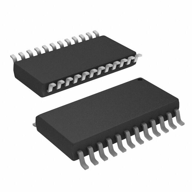
The Si9978 is available in both standard and lead (Pb)-free,
24-pin wide-body SOIC (surface mount) packages, specified
to operate over the industrial (−40 to +85 C) temperature
range.
FUNCTIONAL BLOCK DIAGRAM
V+
Bootstrap Reg.
24
Low-Voltage
Regulator
VDD
1
CAPA
VDD
CAPB
21
22
High-Side
U.V. Lockout
Low-Side
U.V. Lockout
DIR/INA
QS/INB
PWM/ENB
MODE
BRK
EN/ENA
CL/FAULTB
FAULT/FAULTA
RA/CA
RB/CB
23
Charge Pump
Bootstrap Reg.
3
VDD
5
VDD
4
VDD
6
19
Charge Pump
VDD
7
VDD
2
VDD
17
18
VDD
Input
Logic
VDD
20
16
15
8
CAPA
GTA
SA
CAPB
GTB
SB
GBA
GBB
GND
9
11
12
Document Number: 70011
S-40804—Rev. E, 26-Apr-04
One Shot
One Shot
−
+
13
−
+
14
ILA+
ILB+
www.vishay.com
1
�Si9978
Vishay Siliconix
ABSOLUTE MAXIMUM RATINGS
Voltage on pins 2−7 with respect to ground . . . . . . . . . . . −0.3 to VDD + 0.3 V
Voltage on pin 24 . . . . . . . . . . . . . . . . . . . . . . . . . . . . . . . . . . . . . . −0.3 to 50 V
Voltage on pins 17, 19, 21, 23 . . . . . . . . . . . . . . . . . . . . . . . . . . . −0.3 to +60 V
Voltage on pins 18, 22 . . . . . . . . . . . . . . . . . . . . . . . . . . . . . . . . . . . . −2 to 50 V
Operating Temperature (TA) . . . . . . . . . . . . . . . . . . . . . . . . . . . . −40 to +85_C
Storage Temperature . . . . . . . . . . . . . . . . . . . . . . . . . . . . . . . . . . −65 to 150_C
Maximum Junction Temperature (TJ) . . . . . . . . . . . . . . . . . . . . . . . . . . . 150_C
Power Dissipation . . . . . . . . . . . . . . . . . . . . . . . . . . . . . . . . . . . . . . . . 500 mW
RECOMMENDED OPERATING CONDITIONS
V+ . . . . . . . . . . . . . . . . . . . . . . . . . . . . . . . . . . . . . . . . . . . . . . . . . +20 to 40 VDC
RA, RB . . . . . . . . . . . . . . . . . . . . . . . . . . . . . . . . . . . . . . . . . . . . . . . . . . . 100 kW
SPECIFICATIONS
Limits
Test Conditions
Unless Otherwise Specified
Parameter
Symbol
V+ = 20 to 40 V
−40 to 85_C
Mina
Typb
Maxa
16
17.5
3
5
Unit
Power
Supply Voltage Range
V+
20
Logic Voltage
VDD
14.5
Supply Current
I+
IDD = 0 mA
40
V
mA
Inputs (DIR, PWM, EN, QS, MODE, BRK)
High-State
VIH
Low-State
VIL
4.0
High-State Input Current
IIH
VIH = VDD
Low-State Input Current
IIL
VIL = 0 V
1.0
10
−100
−50
−25
14
16
17.5
14
16
18
V
mA
Outputs
Low-Side Gate Drive, High State
VGBH
Low-Side Gate Drive, Low State
VGBL
High-Side Gate Drive, High State
VGTH
High-Side Gate Drive, Low State
VGTL
Low-Side Switching, Rise Time
trL
Low-Side Switching, Fall Time
tfL
High-Side Switching, Rise Time
trH
High-Side Switching, Fall Time
tfH
1
SA,
A B=0V
V
1
110
Rise Time = 1 to 10 V
Fall Time = 10 to 1 V
CL = 600 pF
50
110
ns
50
Break-Before-Make Time
250
FAULT, CL
VOL
IOL = 1 mA
FAULT, CL Leakage Current
IOH
FAULT, CL = VDD
0.2
0.4
V
10
mA
Protection
Low-Side Undervoltage Lockout
Low-Side Hysteresis
High-Side Undervoltage Lockout
UVLL
0.8 VDD
VH
UVLH
0.8
SA, B = 0 V
V
VDD−3.3 V
Current Limit
Comparator Input Bias Current
Comparator Threshold Voltage
IIB
VTH
One Shot Pulse Width
tp
Propagation Delay
tpd
TA = 25_C
−5
−0.2
5
90
100
110
85
115
RA, RB = 100 kW, CA, CB = 100 pF
8
10
12
RA, RB = 100 kW, CA, CB = 0.001 mF
80
100
120
CL = 600 pF
600
mA
mV
ms
ns
Notes:
a. The algebraic convention whereby the most negative value is a minimum and the most positive a maximum, is used in this data sheet.
b. Typical values are for DESIGN AID ONLY, not guaranteed nor subject to production testing.
www.vishay.com
2
Document Number: 70011
S-40804—Rev. E, 26-Apr-04
�Si9978
Vishay Siliconix
TRUTH TABLE� H-BRIDGE MODE
MODE
DIR/
INA
EN/
ENA
QS/
INB
1
1
1
1
1
1
PWM/
ENB
CL/
FAULTB
FAULT/
FAULTA
L
1
1
L
1
1
L
1
1
L
1
1
L
H
1
1
Brake
L
L
L
1
1
Disable
L
L
L
L
X
L
L
L
L
1
0
GBA
GTB
GBB
CL/
FAULTB
FAULT/
FAULTA
BRK
ILA+
ILB+
GTA
GBA
GTB
1
0
L
X
H
L
1
0
0
L
X
L
0
1
1
0
L
X
L
1
0
1
0
0
L
X
L
1
X
1
X
X
1
L
X
L
H
1
X
0
X
X
X
L
X
L
1
X
1
X
X
0
X
1
X
X
X
X
X
X
H
GBB
Condition
Normal
Operation
Overcurrent
Undervoltage
on VDD
TRUTH TABLE� HALF-BRIDGE MODE
MODE
DIR/
INA
EN/
ENA
QS/
INB
PWM/
ENB
BRK
ILA+
ILB+
GTA
0
1
1
X
0
X
L
L
H
L
L
L
1
1
0
0
1
X
0
X
L
L
L
H
L
L
1
1
0
X
0
1
1
X
L
L
L
L
H
L
1
1
0
X
0
0
1
X
L
L
L
L
L
H
1
1
0
X
1
X
X
X
X
L
L
X
X
1
0
X
X
X
1
X
X
X
X
L
L
0
X
X
X
X
X
X
L
L
L
L
Document Number: 70011
S-40804—Rev. E, 26-Apr-04
X
0
Condition
Normal
Operation
Overcurrent on
A
1
Overcurrent on
B
0
Undervoltage
on VDD
www.vishay.com
3
�Si9978
Vishay Siliconix
PIN CONFIGURATION AND ORDERING INFORMATION
SO-24
(Wide Body)
VDD
1
24
V+
EN/ENA
2
23
CAPA
DIR/INA
3
22
SA
PWM/ENB
4
21
GTA
QS/INB
5
20
GBA
MODE
6
19
CAPB
BRK
7
18
SB
CL/FAULTB
8
17
GTB
Si9978DW
FAULT/FAULTA
9
16
GBB
Si9978DW-T1
NC
10
15
GND
RA/CA
11
14
ILB+
RB/CB
12
13
ILA+
ORDERING INFORMATION
Part Number
Lead (Pb)-Free
Part Number
Si9978DW-T1—E3
Temperature
Range
−40
40 to 85_C
Package
SOIC-24
(Wide Body)
Top View
PIN DESCRIPTION
Pin 1: VDD
VDD is an internally generated voltage. It is connected to this
pin to allow connection of a decoupling capacitor. A minimum
of 1 mF is recommended.
As the INA pin, it is the input that controls the “A” half-bridge.
When at logic “1”, the high-side MOSFET is turned on, and
when at logic “0”, the low-side MOSFET is turned on.
Pin 4: PWM/ENB
The EN input allows normal operation when at logic “1”, and
turns all gate drive outputs off when at logic “0”. When the
mode pin is at logic “1”, EN controls the entire H-bridge. When
the mode pin is at logic “0”, this pin becomes the ENABLE pin
for half-bridge A.
With the mode pin at logic “1”, this pin is the PWM input. It
controls the switching of the active diagonal pair. A logic “1”
turns the active MOSFETs on, while a logic “0” turns it off. The
QS input determines whether the bottom or both bottom and
top MOSFETs are switched. When implementing an
anti-phase PWM control, the PWM input is connected to a logic
“1”. When the mode pin is at logic “0”, this pin becomes the
ENABLE pin for half-bridge B.
Pin 3: DIR/INA
Pin 5: QS/INB
The function of this pin is determined by the MODE pin. When
the MODE pin is at logic “1”, it is the DIR pin, and when MODE
is at logic “0”, it is the INA pin.
With the mode pin at logic “1”, this input determines whether
the bottom MOSFETs of the H-bridge or both bottom and top
MOSFETs switch in response to the PWM signal. A logic “1” on
this input enables only the bottom MOSFETs. This is the
default condition as this pin is pulled up internally. When this
pin is pulled to ground, both the bottom and top MOSFETs are
enabled.
Pin 2: EN/ENA
As the DIR input, it is the direction control for the H-bridge, and
determines which diagonal pair of power MOSFETs is active.
A logic “1” turns on GTA and enables GBB, while a logic “0”
turns on GTB and enables GBA. When implementing an
anti-phase PWM control, the DIR input serves as the PWM
input.
www.vishay.com
4
This input controls the B half-bridge when the MODE pin is at
logic “0”. When at logic “1”, the high-side MOSFET is turned on,
and when at logic “0”, the low-side MOSFET is turned on.
Document Number: 70011
S-40804—Rev. E, 26-Apr-04
�Si9978
Vishay Siliconix
PIN DESCRIPTION (CONT’D)
Pin 6: MODE
This input determines whether the Si9978 functions as an
H-bridge or as two independent half-bridges. When the MODE
pin is at logic “1”, the Si9978 functions as an H-bridge, and
when MODE is at logic “0”, it functions as two independent
half-bridges.
Pin 7: BRK
When this input and MODE are at logic “1”, both bottom gate
drives are switched high, turning on the bottom MOSFETs.
When this input is at logic “0”, the Si9978 operates normally.
Pin 8: CL/FAULTB
This is an open drain output which is active low. When the
MODE pin is at logic “1”, this pin functions as CL and indicates
that the H-bridge is in current limit. It stays low for the duration
of the current limit one-shot. With the MODE pin at logic “0”, it
serves as the FAULT output for half-bridge B to indicate when
an undervoltage or overcurrent condition is detected. When
indicating an overcurrent condition, the output stays low for the
duration of the current limit one-shot. The FAULT output resets
automatically when the condition clears.
Pin 9: FAULT/FAULTA
one-shot is triggered when the current limit comparator detects
an overcurrent condition.
Pin 13: ILA+ and Pin 14, ILB+
These are the overcurrent sense inputs. Internally, they are
connected to the noninverting inputs of the current limit
comparators. Externally they are connected to the source(s) of
the low-side MOSFET(s) and the current sense resistor.
Pin 15: GND
The GND pin is the ground return for V+ and the ground
reference for the logic. Also, this is the ground reference input
for the current limit comparators and is connected to the
ground side of the internal 100-mV references. This pin should
be connected directly to the ground side of the current sensing
resistors.
Pin 16: GBB and Pin 20, GBA
These pins drive the gates of the low-side power MOSFETs.
Pin 17: GTB and Pin 21, GTA
These pins drive the gates of the high-side power MOSFETs.
This is an open drain output which is switched low when an
undervoltage or overcurrent condition is detected. When
indicating an overcurrent condition, the output stays low for the
duration of the current limit one-shot. When the MODE pin is
at logic “1”, this pin is the H-bridge FAULT output. With the
MODE pin at logic “0”, it serves as the FAULT output for
half-bridge A. The FAULT output resets automatically when the
condition clears.
Pin 18: SB and Pin 22, SA
Pin 10: NC
No internal connection.
These are the connections for the positive terminals of the
bootstrap capacitors CBA and CBB. A 0.01-mF capacitor can be
used for most applications.
Pin 11: RA/CA
Pin 24: V+
The timing resistor and capacitor for the current limit one-shot
are connected to this pin. The values of the resistor and
capacitor determine the off time set by the one-shot. The
one-shot is triggered when the current limit comparator detects
an overcurrent condition.
This is the only external power supply required for the Si9978,
and must be the same supply used to power the H-bridge it is
driving. The Si9978 powers the low-voltage logic, low-side
gate driver, and bootstrap/ charge pump circuits from
self-contained voltage regulators which require only a
bootstrap capacitor on the CAP pins.
Pin 12: RB/CB
The timing resistor and capacitor for the current limit one-shot
are connected to this pin. The values of the resistor and
capacitor determine the off time set by the one-shot. The
Document Number: 70011
S-40804—Rev. E, 26-Apr-04
These are the source connections of the high-side power
MOSFETs, the drain of the external low-side power MOSFET,
the negative terminal of the bootstrap capacitor, and the output
for each half-bridge.
Pin 19: CAPB and Pin 23, CAPA
No voltage sensing circuitry monitors V+ directly; however, the
low-voltage, internally generated supply and the bootstrap
voltage (which are derived from V+) are directly protected by
undervoltage monitors.
www.vishay.com
5
�Si9978
Vishay Siliconix
APPLICATION CIRCUIT
LITTLE FOOTr
V+
Q3
Q1
C2
C3
C1
C6
U1
1
2
EN
3
DIR
4
PWM
5
QS
6
7
BRK
8
CL
9
FAULT
10
R4
R3
11
12
VCC
R2
100 kW
VDD
V+
EN/ENA
DIR/INA
CAPA
SA
PWM/ENB
GTA
QS/INB
GBA
MODE
CAPB
SB
BRK
CL/FB
GTB
F/FA
GBB
NC
GND
RA/CA
ILB+
RB/CB
ILA+
C7
24
23
C4
A
OUT
22
B
OUT
21
20
19
C5
18
17
Q4
Q2
16
15
14
13
Si9978
R1
C8
GND
FIGURE 1. Basic H-Bridge Circuit
www.vishay.com
6
Document Number: 70011
S-40804—Rev. E, 26-Apr-04
�Package Information
Vishay Siliconix
SOIC (WIDE-BODY): 24-LEAD (POWER IC ONLY)
∅0.06±0.002D
CAVITY NO.
0.303±0.001
24
23
22
21
20
19
18
17
16
15
14
0.334±0.005
13
R0.004
0.295±0.001
0.010
R0.008
R0.009
0.1475±0.001
1
2
3
4
5
6
7
8
9
10
11
12
0.070±0.005
0.055±0.005
0.041±0.001
4_±2_
R0.004
0.032±0.005
PIN 1 INDICATOR
∅0.047X0.007±0.001 dp
SURFACE POLISHED
DETAIL A
0.334±0.005
0.606±0.001
0.291±0.001
0.020x45_
7_(4x)
DETAIL A
0.098±0.002
0.091±0.001
0.050 TYP.
0.017±0.0003
0.006±0.002
R0.004
0.295±0.001
0.406±0.004
ECN: S-40085—Rev. A, 02-Feb-04
DWG: 5930
Document Number: 72825
29-Jan-04
www.vishay.com
1
�Legal Disclaimer Notice
www.vishay.com
Vishay
Disclaimer
ALL PRODUCT, PRODUCT SPECIFICATIONS AND DATA ARE SUBJECT TO CHANGE WITHOUT NOTICE TO IMPROVE
RELIABILITY, FUNCTION OR DESIGN OR OTHERWISE.
Vishay Intertechnology, Inc., its affiliates, agents, and employees, and all persons acting on its or their behalf (collectively,
“Vishay”), disclaim any and all liability for any errors, inaccuracies or incompleteness contained in any datasheet or in any other
disclosure relating to any product.
Vishay makes no warranty, representation or guarantee regarding the suitability of the products for any particular purpose or
the continuing production of any product. To the maximum extent permitted by applicable law, Vishay disclaims (i) any and all
liability arising out of the application or use of any product, (ii) any and all liability, including without limitation special,
consequential or incidental damages, and (iii) any and all implied warranties, including warranties of fitness for particular
purpose, non-infringement and merchantability.
Statements regarding the suitability of products for certain types of applications are based on Vishay's knowledge of typical
requirements that are often placed on Vishay products in generic applications. Such statements are not binding statements
about the suitability of products for a particular application. It is the customer's responsibility to validate that a particular product
with the properties described in the product specification is suitable for use in a particular application. Parameters provided in
datasheets and / or specifications may vary in different applications and performance may vary over time. All operating
parameters, including typical parameters, must be validated for each customer application by the customer's technical experts.
Product specifications do not expand or otherwise modify Vishay's terms and conditions of purchase, including but not limited
to the warranty expressed therein.
Hyperlinks included in this datasheet may direct users to third-party websites. These links are provided as a convenience and
for informational purposes only. Inclusion of these hyperlinks does not constitute an endorsement or an approval by Vishay of
any of the products, services or opinions of the corporation, organization or individual associated with the third-party website.
Vishay disclaims any and all liability and bears no responsibility for the accuracy, legality or content of the third-party website
or for that of subsequent links.
Except as expressly indicated in writing, Vishay products are not designed for use in medical, life-saving, or life-sustaining
applications or for any other application in which the failure of the Vishay product could result in personal injury or death.
Customers using or selling Vishay products not expressly indicated for use in such applications do so at their own risk. Please
contact authorized Vishay personnel to obtain written terms and conditions regarding products designed for such applications.
No license, express or implied, by estoppel or otherwise, to any intellectual property rights is granted by this document or by
any conduct of Vishay. Product names and markings noted herein may be trademarks of their respective owners.
© 2022 VISHAY INTERTECHNOLOGY, INC. ALL RIGHTS RESERVED
Revision: 01-Jan-2022
1
Document Number: 91000
�