SiHD2N80AE
www.vishay.com
Vishay Siliconix
E Series Power MOSFET
FEATURES
D
• Low figure-of-merit (FOM) Ron x Qg
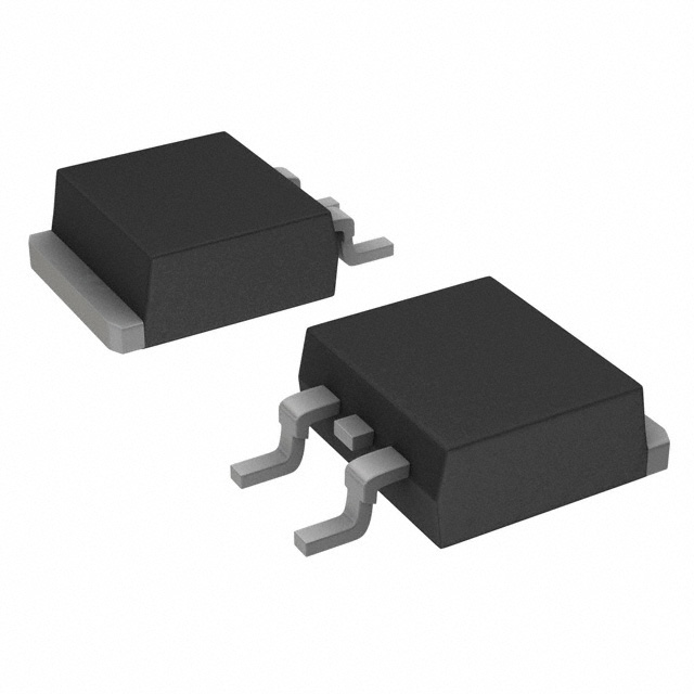
DPAK (TO-252)
• Low effective capacitance (Ciss)
• Reduced switching and conduction losses
D
• Ultra low gate charge (Qg)
G
• Avalanche energy rated (UIS)
S
• Integrated Zener diode ESD protection
G
• Material categorization: for definitions of compliance
please see www.vishay.com/doc?99912
S
N-Channel MOSFET
APPLICATIONS
PRODUCT SUMMARY
• Server and telecom power supplies
VDS (V) at TJ max.
RDS(on) typ. () at 25 °C
850
VGS = 10 V
Qg max. (nC)
• Power factor correction power supplies (PFC)
10.5
Qgs (nC)
3
Qgd (nC)
2
Configuration
• Switch mode power supplies (SMPS)
2.5
• Lighting
- High-intensity discharge (HID)
- Fluorescent ballast lighting
Single
• Industrial
- Welding
- Induction heating
- Motor drives
- Battery chargers
- Renewable energy
- Solar (PV inverters)
ORDERING INFORMATION
Package
DPAK (TO-252)
Lead (Pb)-free and halogen-free
SiHD2N80AE-GE3
ABSOLUTE MAXIMUM RATINGS (TC = 25 °C, unless otherwise noted)
PARAMETER
SYMBOL
LIMIT
Drain-source voltage
VDS
800
Gate-source voltage
VGS
± 30
Continuous drain current (TJ = 150 °C)
VGS at 10 V
TC = 25 °C
TC = 100 °C
Pulsed drain current a
ID
UNIT
V
2.9
1.8
A
IDM
3.6
0.5
W/°C
Single pulse avalanche energy b
EAS
14.1
mJ
Maximum power dissipation
PD
62.5
W
TJ, Tstg
-55 to +150
°C
Linear derating factor
Operating junction and storage temperature range
Drain-source voltage slope
TJ = 125 °C
Reverse diode dv/dt d
Soldering recommendations (peak temperature) c
For 10 s
dv/dt
70
0.1
260
V/ns
°C
Notes
a. Repetitive rating; pulse width limited by maximum junction temperature
b. VDD = 140 V, starting TJ = 25 °C, L = 28.2 mH, Rg = 25 , IAS = 1 A
c. 1.6 mm from case
d. ISD ID, di/dt = 100 A/μs, starting TJ = 25 °C
S19-0120-Rev. A, 04-Feb-2019
Document Number: 92238
1
For technical questions, contact: hvm@vishay.com
THIS DOCUMENT IS SUBJECT TO CHANGE WITHOUT NOTICE. THE PRODUCTS DESCRIBED HEREIN AND THIS DOCUMENT
ARE SUBJECT TO SPECIFIC DISCLAIMERS, SET FORTH AT www.vishay.com/doc?91000
�SiHD2N80AE
www.vishay.com
Vishay Siliconix
THERMAL RESISTANCE RATINGS
PARAMETER
SYMBOL
TYP.
MAX.
Maximum junction-to-ambient
RthJA
-
62
Maximum junction-to-case (drain)
RthJC
-
2.0
UNIT
°C/W
SPECIFICATIONS (TJ = 25 °C, unless otherwise noted)
PARAMETER
SYMBOL
TEST CONDITIONS
MIN.
TYP.
MAX.
UNIT
Static
Drain-source breakdown voltage
VDS temperature coefficient
Gate-source threshold voltage (N)
VDS
VGS = 0 V, ID = 250 μA
800
-
-
V
VDS/TJ
Reference to 25 °C, ID = 1 mA
-
0.8
-
V/°C
VGS(th)
VDS = VGS, ID = 250 μA
2.0
-
4.0
V
VGS = ± 20 V
-
-
± 10
VGS = ± 30 V
-
-
± 50
VDS = 800 V, VGS = 0 V
-
-
1
VDS = 640 V, VGS = 0 V, TJ = 125 °C
-
-
10
Gate-source leakage
IGSS
Zero gate voltage drain current
IDSS
μA
μA
-
2.5
2.9
gfs
VDS = 30 V, ID = 1 A
-
0.6
-
S
Input capacitance
Ciss
180
-
Coss
-
10
-
Reverse transfer capacitance
Crss
VGS = 0 V,
VDS = 100 V,
f = 1 MHz
-
Output capacitance
-
1
-
Effective output capacitance, energy
related a
Co(er)
-
7
-
Effective output capacitance, time
related b
Co(tr)
-
42
-
-
7
10.5
-
3
-
Drain-source on-state resistance
Forward transconductance a
RDS(on)
VGS = 10 V
ID = 0.5 A
Dynamic
pF
VDS = 0 V to 480 V, VGS = 0 V
Total gate charge
Qg
Gate-source charge
Qgs
VGS = 10 V
ID = 1.5 A, VDS = 640 V
Gate-drain charge
Qgd
-
2
-
Turn-on delay time
td(on)
-
13
26
Rise time
Turn-off delay time
tr
td(off)
Fall time
tf
Gate input resistance
Rg
VDD = 640 V, ID = 1.5 A,
VGS = 10 V, Rg = 4.7
-
8
16
-
10
20
-
23
46
f = 1 MHz, open drain
2.0
5.2
10.4
-
-
2.9
-
-
3.6
nC
ns
Drain-Source Body Diode Characteristics
Continuous source-drain diode current
IS
Pulsed diode forward current
ISM
Diode forward voltage
VSD
Reverse recovery time
trr
Reverse recovery charge
Qrr
Reverse recovery current
IRRM
MOSFET symbol
showing the
integral reverse
p - n junction diode
D
A
G
TJ = 25 °C, IS = 1 A, VGS = 0 V
TJ = 25 °C, IF = IS = 1 A,
di/dt = 100 A/μs, VR = 25 V
S
-
-
1.2
V
-
313
626
ns
-
0.7
1.4
μC
-
3.8
-
A
Notes
a. Coss(er) is a fixed capacitance that gives the same energy as Coss while VDS is rising from 0 V to 480 V VDSS
b. Coss(tr) is a fixed capacitance that gives the same charging time as Coss while VDS is rising from 0 V to 480 V VDSS
S19-0120-Rev. A, 04-Feb-2019
Document Number: 92238
2
For technical questions, contact: hvm@vishay.com
THIS DOCUMENT IS SUBJECT TO CHANGE WITHOUT NOTICE. THE PRODUCTS DESCRIBED HEREIN AND THIS DOCUMENT
ARE SUBJECT TO SPECIFIC DISCLAIMERS, SET FORTH AT www.vishay.com/doc?91000
�SiHD2N80AE
www.vishay.com
Vishay Siliconix
TYPICAL CHARACTERISTICS (25 °C, unless otherwise noted)
Axis Title
8V
1000
2
7V
100
1
6V
5V
2.5
0
5
10
15
1000
2.0
1.5
VGS = 10 V
1.0
10
0
20
-60 -40 -20 0
20 40 60 80 100 120 140 160
VDS - Drain-to-Source Voltage (V)
TJ - Junction Temperature (°C)
Fig. 1 - Typical Output Characteristics
Fig. 4 - Normalized On-Resistance vs. Temperature
Axis Title
Axis Title
2.4
10000
TJ = 150 °C
15 V
14 V
13 V
12 V
11 V
10 V
9V
8V
7V
1000
6V
100
0.6
Ciss
1000
100
1st line
2nd line
1.2
VGS = 0 V, f = 1 MHz
Ciss = Cgs + Cgd, Cds shorted
Crss = Cgd
Coss = Cds + Cgd
1000
2nd line
C - Capacitance (pF)
1.8
10000
10 000
1st line
2nd line
2nd line
ID - Drain-to-Source Current (A)
100
0.5
10
0
10000
ID = 1 A
1st line
2nd line
TJ = 25 °C
RDS(on) - Drain-to-Source On-Resistance
(Normalized)
15 V
14 V
13 V
12 V
11 V
10 V
9V
3
Axis Title
3.0
10000
1st line
2nd line
2nd line
ID - Drain-to-Source Current (A)
4
Coss
10
100
Crss
1
5V
5
10
15
20
0
100
200
400
500
600
VDS - Drain-to-Source Voltage (V)
VDS - Drain-to-Source Voltage (V)
Fig. 2 - Typical Output Characteristics
Fig. 5 - Typical Capacitance vs. Drain-to-Source Voltage
Axis Title
Axis Title
10 000
10000
TJ = 25 °C
3
2
1st line
2nd line
1000
TJ = 150 °C
100
1
2nd line
Coss - Output Capacitance (pF)
4
2nd line
ID - Drain-to-Source Current (A)
300
2
1000
1.5
100
1
Eoss
Coss
10
0.5
VDS = 28.8 V
10
0
0
5
10
15
20
1
0
0
100
200
300
400
500
VGS - Gate-to-Source Voltage (V)
VDS - Drain-to-Source Voltage (V)
Fig. 3 - Typical Transfer Characteristics
Fig. 6 - Coss and Eoss vs. VDS
S19-0120-Rev. A, 04-Feb-2019
Eoss - Output Capacitance Stored Energy (µJ)
2nd line
0
10
0.1
10
0
600
Document Number: 92238
3
For technical questions, contact: hvm@vishay.com
THIS DOCUMENT IS SUBJECT TO CHANGE WITHOUT NOTICE. THE PRODUCTS DESCRIBED HEREIN AND THIS DOCUMENT
ARE SUBJECT TO SPECIFIC DISCLAIMERS, SET FORTH AT www.vishay.com/doc?91000
�SiHD2N80AE
www.vishay.com
Vishay Siliconix
Axis Title
Axis Title
10000
3
10000
VDS = 640 V
VDS = 400 V
VDS = 160 V
6
100
3
1000
2
1st line
2nd line
1000
2nd line
ID - Drain Current (A)
2.5
9
1st line
2nd line
2nd line
VGS - Gate-to-Source Voltage (V)
12
1.5
100
1
0.5
0
2
4
6
10
0
10
0
25
8
50
75
100
125
150
Qg - Total Gate Charge (nC)
TC - Case Temperature (°C)
Fig. 7 - Typical Gate Charge vs. Gate-to-Source Voltage
Fig. 10 - Maximum Drain Current vs. Case Temperature
Axis Title
1000
TJ = 25 °C
1
100
VGS = 0 V
10
0.1
0.2
0.4
0.6
0.8
1.0
1.2
1.4
10000
1025
1000
975
1000
950
1st line
2nd line
TJ = 150 °C
1st line
2nd line
2nd line
ISD - Reverse Drain Current (A)
10000
2nd line
VDS - Drain-to-Source Breakdown Voltage (V)
Axis Title
10
925
900
100
875
850
825
ID = 250 µA
10
800
-60 -40 -20 0
20 40 60 80 100 120 140 160
VSD - Source-Drain Voltage (V)
TJ - Junction Temperature (°C)
Fig. 8 - Typical Source-Drain Diode Forward Voltage
Fig. 11 - Temperature vs. Drain-to-Source Voltage
Axis Title
Operation in this area
limited by RDS(on)
10000
IDM limited
1000
1
Limited by RDS(on) a
1st line
2nd line
2nd line
ID - Drain Current (A)
10
100 µs
100
0.1
1 ms
TC = 25 °C,
TJ = 150 °C,
single pulse
10 ms
BVDSS limited
0.01
1
10
100
1000
10
10000
VDS - Drain-to-Source Voltage (V)
Fig. 9 - Maximum Safe Operating Area
Note
a. VGS > minimum VGS at which RDS(on) is specified
S19-0120-Rev. A, 04-Feb-2019
Document Number: 92238
4
For technical questions, contact: hvm@vishay.com
THIS DOCUMENT IS SUBJECT TO CHANGE WITHOUT NOTICE. THE PRODUCTS DESCRIBED HEREIN AND THIS DOCUMENT
ARE SUBJECT TO SPECIFIC DISCLAIMERS, SET FORTH AT www.vishay.com/doc?91000
�SiHD2N80AE
www.vishay.com
Vishay Siliconix
Axis Title
1
10000
0.2
0.1
0.05
1000
1st line
2nd line
Normalized Effective Transient
Thermal Impedance
Duty cycle = 0.5
0.02
0.1
Single pulse
100
10
0.01
0.0001
0.001
0.01
0.1
1
Pulse Time (s)
Fig. 12 - Normalized Transient Thermal Impedance, Junction-to-Case
RD
VDS
VDS
tp
VGS
D.U.T.
VDD
Rg
+
- VDD
VDS
10 V
Pulse width ≤ 1 μs
Duty factor ≤ 0.1 %
IAS
Fig. 13 - Switching Time Test Circuit
Fig. 16 - Unclamped Inductive Waveforms
VDS
Qg
10 V
90 %
Qgs
10 %
VGS
Qgd
VG
td(on)
td(off)
tr
tf
Charge
Fig. 14 - Switching Time Waveforms
Fig. 17 - Basic Gate Charge Waveform
Current regulator
Same type as D.U.T.
L
VDS
Vary tp to obtain
required IAS
50 kΩ
12 V
D.U.T.
Rg
0.2 μF
0.3 μF
+
- VDD
+
D.U.T.
IAS
10 V
tp
0.01 Ω
-
VDS
VGS
3 mA
Fig. 15 - Unclamped Inductive Test Circuit
IG
ID
Current sampling resistors
Fig. 18 - Gate Charge Test Circuit
S19-0120-Rev. A, 04-Feb-2019
Document Number: 92238
5
For technical questions, contact: hvm@vishay.com
THIS DOCUMENT IS SUBJECT TO CHANGE WITHOUT NOTICE. THE PRODUCTS DESCRIBED HEREIN AND THIS DOCUMENT
ARE SUBJECT TO SPECIFIC DISCLAIMERS, SET FORTH AT www.vishay.com/doc?91000
�SiHD2N80AE
www.vishay.com
Vishay Siliconix
Peak Diode Recovery dv/dt Test Circuit
+
D.U.T.
Circuit layout considerations
• Low stray inductance
• Ground plane
• Low leakage inductance
current transformer
3
+
2
-
-
4
+
1
Rg
•
•
•
•
1 Driver gate drive
Period
P.W.
+
V
- DD
dv/dt controlled by Rg
Driver same type as D.U.T.
ISD controlled by duty factor “D”
D.U.T. - device under test
D=
P.W.
Period
V GS = 10 V a
2
D.U.T. ISD waveform
Reverse
recovery
current
3 D.U.T. VDS
Body diode forward
current
di/dt
waveform
Diode recovery
dv/dt
Re-applied
voltage
V DD
Body diode forward drop
4 Inductor current
Ripple ≤ 5 %
ISD
Note
a. VGS = 5 V for logic level devices
Fig. 19 - For N-Channel
Vishay Siliconix maintains worldwide manufacturing capability. Products may be manufactured at one of several qualified locations. Reliability data for Silicon
Technology and Package Reliability represent a composite of all qualified locations. For related documents such as package/tape drawings, part marking, and
reliability data, see www.vishay.com/ppg?92238.
S19-0120-Rev. A, 04-Feb-2019
Document Number: 92238
6
For technical questions, contact: hvm@vishay.com
THIS DOCUMENT IS SUBJECT TO CHANGE WITHOUT NOTICE. THE PRODUCTS DESCRIBED HEREIN AND THIS DOCUMENT
ARE SUBJECT TO SPECIFIC DISCLAIMERS, SET FORTH AT www.vishay.com/doc?91000
�Package Information
Vishay Siliconix
TO-252AA (HIGH VOLTAGE)
E
b3
E1
L3
D1
D
H
L4
b2
b
A
c2
e
A1
L1
L
c
θ
L2
MILLIMETERS
INCHES
DIM.
MIN.
MAX.
MIN.
MAX.
E
6.40
6.73
0.252
0.265
L
1.40
1.77
0.055
L1
2.743 REF
L2
0.070
0.108 REF
0.508 BSC
0.020 BSC
L3
0.89
1.27
0.035
0.050
L4
0.64
1.01
0.025
0.040
D
6.00
6.22
0.236
0.245
H
9.40
10.40
0.370
0.409
b
0.64
0.88
0.025
0.035
b2
0.77
1.14
0.030
0.045
b3
5.21
5.46
0.205
e
2.286 BSC
0.215
0.090 BSC
A
2.20
2.38
0.087
A1
0.00
0.13
0.000
0.094
0.005
c
0.45
0.60
0.018
0.024
c2
0.45
0.58
0.018
0.023
D1
5.30
-
0.209
-
E1
4.40
-
0.173
-
θ
0'
10'
0'
10'
ECN: S-81965-Rev. A, 15-Sep-08
DWG: 5973
Notes
1. Package body sizes exclude mold flash, protrusion or gate burrs. Mold flash, protrusion or gate burrs shall not exceed 0.10 mm per side.
2. Package body sizes determined at the outermost extremes of the plastic body exclusive of mold flash, gate burrs and interlead flash, but
including any mismatch between the top and bottom of the plastic body.
3. The package top may be smaller than the package bottom.
4. Dimension "b" does not include dambar protrusion. Allowable dambar protrusion shall be 0.10 mm total in excess of "b" dimension at maximum
material condition. The dambar cannot be located on the lower radius of the foot.
Document Number: 91344
Revision: 15-Sep-08
www.vishay.com
1
�Application Note 826
Vishay Siliconix
RECOMMENDED MINIMUM PADS FOR DPAK (TO-252)
0.224
0.243
0.087
(2.202)
0.090
(2.286)
(10.668)
0.420
(6.180)
(5.690)
0.180
0.055
(4.572)
(1.397)
Recommended Minimum Pads
Dimensions in Inches/(mm)
Return to Index
Return to Index
APPLICATION NOTE
Document Number: 72594
Revision: 21-Jan-08
www.vishay.com
3
�Legal Disclaimer Notice
www.vishay.com
Vishay
Disclaimer
ALL PRODUCT, PRODUCT SPECIFICATIONS AND DATA ARE SUBJECT TO CHANGE WITHOUT NOTICE TO IMPROVE
RELIABILITY, FUNCTION OR DESIGN OR OTHERWISE.
Vishay Intertechnology, Inc., its affiliates, agents, and employees, and all persons acting on its or their behalf (collectively,
“Vishay”), disclaim any and all liability for any errors, inaccuracies or incompleteness contained in any datasheet or in any other
disclosure relating to any product.
Vishay makes no warranty, representation or guarantee regarding the suitability of the products for any particular purpose or
the continuing production of any product. To the maximum extent permitted by applicable law, Vishay disclaims (i) any and all
liability arising out of the application or use of any product, (ii) any and all liability, including without limitation special,
consequential or incidental damages, and (iii) any and all implied warranties, including warranties of fitness for particular
purpose, non-infringement and merchantability.
Statements regarding the suitability of products for certain types of applications are based on Vishay's knowledge of typical
requirements that are often placed on Vishay products in generic applications. Such statements are not binding statements
about the suitability of products for a particular application. It is the customer's responsibility to validate that a particular product
with the properties described in the product specification is suitable for use in a particular application. Parameters provided in
datasheets and / or specifications may vary in different applications and performance may vary over time. All operating
parameters, including typical parameters, must be validated for each customer application by the customer's technical experts.
Product specifications do not expand or otherwise modify Vishay's terms and conditions of purchase, including but not limited
to the warranty expressed therein.
Hyperlinks included in this datasheet may direct users to third-party websites. These links are provided as a convenience and
for informational purposes only. Inclusion of these hyperlinks does not constitute an endorsement or an approval by Vishay of
any of the products, services or opinions of the corporation, organization or individual associated with the third-party website.
Vishay disclaims any and all liability and bears no responsibility for the accuracy, legality or content of the third-party website
or for that of subsequent links.
Except as expressly indicated in writing, Vishay products are not designed for use in medical, life-saving, or life-sustaining
applications or for any other application in which the failure of the Vishay product could result in personal injury or death.
Customers using or selling Vishay products not expressly indicated for use in such applications do so at their own risk. Please
contact authorized Vishay personnel to obtain written terms and conditions regarding products designed for such applications.
No license, express or implied, by estoppel or otherwise, to any intellectual property rights is granted by this document or by
any conduct of Vishay. Product names and markings noted herein may be trademarks of their respective owners.
© 2021 VISHAY INTERTECHNOLOGY, INC. ALL RIGHTS RESERVED
Revision: 09-Jul-2021
1
Document Number: 91000
�