SiJ188DP
www.vishay.com
Vishay Siliconix
N-Channel 60 V (D-S) MOSFET
FEATURES
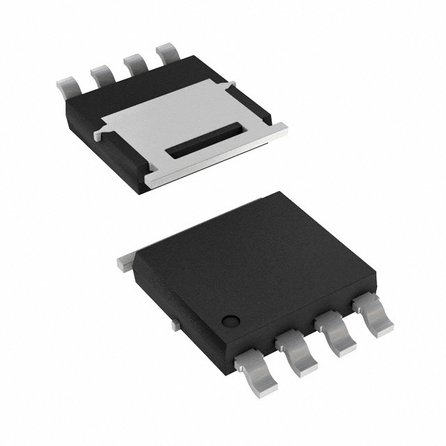
PowerPAK® SO-8L Single
• TrenchFET® Gen IV power MOSFET
• Very low RDS - Qg figure-of-merit (FOM)
• Tuned for the lowest RDS - Qoss FOM
D
6.
15
m
m
m
1
13
m
4
G
5.
Top View
3
S
2
S
• 100 % Rg and UIS tested
1
S
• Material categorization: for definitions of
compliance please see www.vishay.com/doc?99912
APPLICATIONS
Bottom View
PRODUCT SUMMARY
VDS (V)
RDS(on) max. () at VGS = 10 V
RDS(on) max. () at VGS = 7.5 V
Qg typ. (nC)
ID (A)
Configuration
D
• Synchronous rectification
• Primary side switch
60
0.00385
0.00490
22
92.4
Single
• DC/DC converter
G
• Motor drive switch
S
N-Channel MOSFET
ORDERING INFORMATION
Package
Lead (Pb)-free and halogen-free
PowerPAK SO-8L
SiJ188DP-T1-GE3
ABSOLUTE MAXIMUM RATINGS (TA = 25 °C, unless otherwise noted)
PARAMETER
Drain-source voltage
Gate-source voltage
Continuous drain current (TJ = 150 °C)
SYMBOL
VDS
VGS
TC = 25 °C
TC = 70 °C
TA = 25 °C
TA = 70 °C
Pulsed drain current (t = 100 μs)
ID
IDM
Continuous source-drain diode current
TC = 25 °C
TA = 25 °C
IS
Single pulse avalanche current
Single pulse avalanche energy
L = 0.1 mH
IAS
EAS
TC = 25 °C
TC = 70 °C
Maximum power dissipation
TA = 25 °C
TA = 70 °C
Operating junction and storage temperature range
Soldering recommendations (peak temperature) c
PD
TJ, Tstg
LIMIT
60
± 20
92.4
73.9
25.5 b, c
20.3 b, c
150
59.7
4.5 b, c
25
31.25
65.7
42
5 b, c
3.2 b, c
-55 to +150
260
UNIT
V
A
mJ
W
°C
THERMAL RESISTANCE RATINGS
PARAMETER
SYMBOL
TYPICAL
MAXIMUM
UNIT
Maximum junction-to-ambient b
t 10 s
RthJA
20
25
°C/W
1.6
1.9
Maximum junction-to-case (drain)
Steady state
RthJC
Notes
a. Package limited
b. Surface mounted on 1" x 1" FR4 board
c. t = 10 s
d. See solder profile (www.vishay.com/doc?73257). The PowerPAK SO-8 is a leadless package. The end of the lead terminal is exposed copper
(not plated) as a result of the singulation process in manufacturing. A solder fillet at the exposed copper tip cannot be guaranteed and is not
required to ensure adequate bottom side solder interconnection
e. Rework conditions: manual soldering with a soldering iron is not recommended for leadless components
f. Maximum under steady state conditions is 70 °C/W
g. TC = 25 °C
S18-0822-Rev. A, 13-Aug-2018
Document Number: 76828
1
For technical questions, contact: pmostechsupport@vishay.com
THIS DOCUMENT IS SUBJECT TO CHANGE WITHOUT NOTICE. THE PRODUCTS DESCRIBED HEREIN AND THIS DOCUMENT
ARE SUBJECT TO SPECIFIC DISCLAIMERS, SET FORTH AT www.vishay.com/doc?91000
�SiJ188DP
www.vishay.com
Vishay Siliconix
SPECIFICATIONS (TJ = 25 °C, unless otherwise noted)
PARAMETER
SYMBOL
TEST CONDITIONS
MIN.
TYP.
MAX.
UNIT
V
Static
Drain-source breakdown voltage
VDS
VGS = 0 V, ID = 250 μA
60
-
-
VDS/TJ
ID = 10 mA
-
34
-
VGS(th) temperature coefficient
VGS(th)/TJ
ID = 250 μA
-
-6.7
-
Gate-source threshold voltage
VDS temperature coefficient
mV/°C
VGS(th)
VDS = VGS, ID = 250 μA
2
-
3.6
V
Gate-source leakage
IGSS
VDS = 0 V, VGS = ± 20 V
-
-
100
nA
Zero gate voltage drain current
IDSS
On-state drain current a
ID(on)
Drain-source on-state resistance a
Forward transconductance a
RDS(on)
gfs
VDS = 60 V, VGS = 0 V
-
-
1
VDS = 60 V, VGS = 0 V, TJ = 70 °C
-
-
15
VDS 10 V, VGS = 10 V
40
-
-
A
VGS = 10 V, ID = 10 A
-
0.00320
0.00385
VGS = 7.5 V, ID = 10 A
-
0.00380
0.00490
VDS = 15 V, ID = 10 A
-
41
-
-
1920
-
-
530
-
-
26
-
-
29
44
-
22
33
-
6.8
-
-
5
-
μA
S
Dynamic b
Input capacitance
Ciss
Output capacitance
Coss
Reverse transfer capacitance
Crss
Total gate charge
Qg
Gate-source charge
Qgs
Gate-drain charge
Qgd
Output charge
Qoss
VDS = 30 V, VGS = 0 V
-
32.5
-
Gate resistance
Rg
f = 1 MHz
0.3
0.9
1.5
-
13
26
-
6
12
-
22
44
Turn-on delay time
Rise time
Turn-off delay time
Fall time
Turn-on delay time
Rise time
Turn-off delay time
Fall time
VDS = 30 V, VGS = 0 V, f = 1 MHz
VDS = 30 V, VGS = 10 V, ID = 10 A
VDS = 30 V, VGS = 7.5 V, ID = 10 A
td(on)
tr
td(off)
VDD = 30 V, RL = 3 , ID 10 A,
VGEN = 10 V, Rg = 1
tf
-
6
12
td(on)
-
16
32
-
8
16
-
20
40
-
8
16
tr
td(off)
VDD = 30 V, RL = 3 , ID 10 A,
VGEN = 7.5 V, Rg = 1
tf
pF
nC
ns
Drain-Source Body Diode Characteristics
Continuous source-drain diode current
IS
Pulse diode forward current
ISM
Body diode voltage
VSD
Body diode reverse recovery time
trr
Body diode reverse recovery charge
Qrr
Reverse recovery fall time
ta
Reverse recovery rise time
tb
TC = 25 °C
IS = 5 A, VGS = 0 V
IF = 10 A, di/dt = 100 A/μs,
TJ = 25 °C
-
-
59.7
-
-
150
-
0.76
1.1
V
-
46
92
ns
-
44
88
nC
-
21
-
-
25
-
A
ns
Notes
a. Pulse test; pulse width 300 μs, duty cycle 2 %
b. Guaranteed by design, not subject to production testing
Stresses beyond those listed under “Absolute Maximum Ratings” may cause permanent damage to the device. These are stress ratings only, and functional operation
of the device at these or any other conditions beyond those indicated in the operational sections of the specifications is not implied. Exposure to absolute maximum
rating conditions for extended periods may affect device reliability.
S18-0822-Rev. A, 13-Aug-2018
Document Number: 76828
2
For technical questions, contact: pmostechsupport@vishay.com
THIS DOCUMENT IS SUBJECT TO CHANGE WITHOUT NOTICE. THE PRODUCTS DESCRIBED HEREIN AND THIS DOCUMENT
ARE SUBJECT TO SPECIFIC DISCLAIMERS, SET FORTH AT www.vishay.com/doc?91000
�SiJ188DP
www.vishay.com
Vishay Siliconix
TYPICAL CHARACTERISTICS (25 °C, unless otherwise noted)
125
100
VGS = 10 V thru 6V
100
2nd line
ID - Drain Current (A)
2nd line
ID - Drain Current (A)
80
VGS = 5 V
60
40
20
75
TC = 125 °C
50
TC = 25 °C
25
VGS = 4 V
TC = -55 °C
VGS = 3 V
0
2
4
6
8
0
10
2
4
Output Characteristics
Transfer Characteristics
10000
Ciss
0.0032
100
VGS = 10 V
0.0026
1000
1500
Coss
1000
100
500
0.002
40
60
80
Crss
0
10
20
1st line
2nd line
1000
0.0038
2nd line
C - Capacitance (pF)
2000
VGS = 7.5 V
1st line
2nd line
2nd line
RDS(on) - On-Resistance (Ω)
2500
10000
0.0044
10
0
100
12
24
36
48
ID - Drain Current (A)
2nd line
VDS - Drain-to-Source Voltage (V)
2nd line
On-Resistance vs. Drain Current and Gate Voltage
Capacitance
Axis Title
2.0
ID = 10 A
8
1000
1st line
2nd line
6
VDS = 25 V, 50 V, 75 V
4
100
2
0
10
12
18
24
30
2nd line
RDS(on) - On-Resistance (Normalized)
10000
6
60
Axis Title
10
0
10
Axis Title
Axis Title
2nd line
VGS - Gate-to-Source Voltage (V)
8
VGS - Gate-to-Source Voltage (V)
2nd line
0.0050
0
6
VDS - Drain-to-Source Voltage (V)
2nd line
10000
ID = 10 A
VGS = 10 V
1.7
1000
1.4
VGS = 7.5 V
1.1
100
0.8
0.5
10
-50
-25
0
25
50
75
100 125 150
Qg - Total Gate Charge (nC)
2nd line
TJ - Junction Temperature (°C)
2nd line
Gate Charge
On-Resistance vs. Junction Temperature
S18-0822-Rev. A, 13-Aug-2018
1st line
2nd line
0
0
Document Number: 76828
3
For technical questions, contact: pmostechsupport@vishay.com
THIS DOCUMENT IS SUBJECT TO CHANGE WITHOUT NOTICE. THE PRODUCTS DESCRIBED HEREIN AND THIS DOCUMENT
ARE SUBJECT TO SPECIFIC DISCLAIMERS, SET FORTH AT www.vishay.com/doc?91000
�SiJ188DP
www.vishay.com
Vishay Siliconix
TYPICAL CHARACTERISTICS (25 °C, unless otherwise noted)
Axis Title
Axis Title
10000
0.2
2nd line
VGS(th) - Variance (V)
1000
TJ = 150 °C
TJ = 25 °C
1
100
1000
-0.2
ID = 5 mA
-0.6
100
0.1
ID = 250 μA
-1.0
0.01
-1.4
10
0
0.3
0.6
0.9
1.2
10
-50
1.5
-25
0
25
50
75
100 125 150
VSD - Source-to-Drain Voltage (V)
2nd line
TJ - Temperature (°C)
2nd line
Source-Drain Diode Forward Voltage
Threshold Voltage
Axis Title
Axis Title
0.030
ID = 10 A
0.024
10000
250
10000
200
1000
2nd line
Power (W)
1000
0.012
150
1st line
2nd line
0.018
1st line
2nd line
2nd line
RDS(on) - On-Resistance (Ω)
1st line
2nd line
10
1st line
2nd line
2nd line
IS - Source Current (A)
0.6
10000
100
100
100
TJ = 125 °C
100
0.006
50
TJ = 25 °C
0
10
2
4
6
8
10
0
0.001
10
0.01
0.1
1
10
VGS - Gate-to-Source Voltage (V)
2nd line
Time (s)
2nd line
On-Resistance vs. Gate-to-Source Voltage
Single Pulse Power, Junction-to-Ambient
Axis Title
10000
1000
IDM limited
ID limited
100 μs
1000
10
1 ms
Limited by
RDS(on) (1)
1
10 ms
100 ms
1s
0.1
1st line
2nd line
2nd line
ID - Drain Current (A)
100
100
10 s
DC
0.01
TA = 25 °C
Single pulse
0.001
0.01
(1)
BVDSS limited
10
0.1
1
10
100
VDS - Drain-to-Source Voltage (V)
VGS > minimum VGS at which RDS(on) is specified
Safe Operating Area, Junction-to-Ambient
S18-0822-Rev. A, 13-Aug-2018
Document Number: 76828
4
For technical questions, contact: pmostechsupport@vishay.com
THIS DOCUMENT IS SUBJECT TO CHANGE WITHOUT NOTICE. THE PRODUCTS DESCRIBED HEREIN AND THIS DOCUMENT
ARE SUBJECT TO SPECIFIC DISCLAIMERS, SET FORTH AT www.vishay.com/doc?91000
�SiJ188DP
www.vishay.com
Vishay Siliconix
TYPICAL CHARACTERISTICS (25 °C, unless otherwise noted)
Axis Title
100
10000
1000
60
1st line
2nd line
2nd line
ID - Drain Current (A)
80
40
100
20
0
10
0
25
50
75
100
125
150
TC - Case Temperature (°C)
2nd line
Current Derating a
Axis Title
Axis Title
80
10000
2.5
64
10000
2
1.5
1st line
2nd line
32
2nd line
Power (W)
1000
1st line
2nd line
2nd line
Power (W)
1000
48
1
100
16
100
0.5
0
10
0
25
50
75
100
125
150
0
10
0
25
50
75
100
125
TC - Case Temperature (°C)
2nd line
TA - Ambient Temperature (°C)
2nd line
Power, Junction-to-Case
Power, Junction-to-Ambient
150
Note
a. The power dissipation PD is based on TJ max. = 150 °C, using junction-to-case thermal resistance, and is more useful in settling the upper
dissipation limit for cases where additional heatsinking is used. It is used to determine the current rating, when this rating falls below the
package limit.
S18-0822-Rev. A, 13-Aug-2018
Document Number: 76828
5
For technical questions, contact: pmostechsupport@vishay.com
THIS DOCUMENT IS SUBJECT TO CHANGE WITHOUT NOTICE. THE PRODUCTS DESCRIBED HEREIN AND THIS DOCUMENT
ARE SUBJECT TO SPECIFIC DISCLAIMERS, SET FORTH AT www.vishay.com/doc?91000
�SiJ188DP
www.vishay.com
Vishay Siliconix
TYPICAL CHARACTERISTICS (25 °C, unless otherwise noted)
Axis Title
10000
Duty Cycle = 0.5
Notes:
0.2
1000
1st line
2nd line
Normalized Effective Transient
Thermal Impedance
1
PDM
0.1
0.1
t1
t2
t
1. Duty cycle, D = 1
t2
2. Per unit base = RthJA = 70 °C/W
0.05
0.02
3. TJM - TA = PDMZthJA
Single pulse
0.01
0.0001
0.001
0.01
100
(t)
4. Surface mounted
0.1
1
10
100
10
1000
Square Wave Pulse Duration (s)
2nd line
Normalized Thermal Transient Impedance, Junction-to-Ambient
Axis Title
10000
Duty Cycle = 0.5
0.2
1000
0.1
1st line
2nd line
Normalized Effective Transient
Thermal Impedance
1
0.05
0.1
0.02
100
Single pulse
0.01
0.0001
10
0.001
0.01
0.1
1
Square Wave Pulse Duration (s)
2nd line
Normalized Thermal Transient Impedance, Junction-to-Case
Vishay Siliconix maintains worldwide manufacturing capability. Products may be manufactured at one of several qualified locations. Reliability data for Silicon
Technology and Package Reliability represent a composite of all qualified locations. For related documents such as package / tape drawings, part marking, and
reliability data, see www.vishay.com/ppg?76828.
S18-0822-Rev. A, 13-Aug-2018
Document Number: 76828
6
For technical questions, contact: pmostechsupport@vishay.com
THIS DOCUMENT IS SUBJECT TO CHANGE WITHOUT NOTICE. THE PRODUCTS DESCRIBED HEREIN AND THIS DOCUMENT
ARE SUBJECT TO SPECIFIC DISCLAIMERS, SET FORTH AT www.vishay.com/doc?91000
�PAD Pattern
www.vishay.com
Vishay Siliconix
RECOMMENDED MINIMUM PAD FOR PowerPAK® SO-8L SINGLE
5.000
(0.197)
0.510
(0.020)
2.310
(0.091)
4.061
(0.160)
0.595
(0.023)
6.250
(0.246)
8.250
(0.325)
3.630
(0.143)
0.610
(0.024)
0.410
(0.016)
2.715
(0.107)
0.860
(0.034)
1.291
(0.051)
0.710
(0.028)
0.820
(0.032)
1.905
(0.075)
1.270
(0.050)
7.250
(0.285)
Recommended Minimum Pads
Dimensions in mm (inches)
Revision: 07-Feb-12
1
Document Number: 63818
THIS DOCUMENT IS SUBJECT TO CHANGE WITHOUT NOTICE. THE PRODUCTS DESCRIBED HEREIN AND THIS DOCUMENT
ARE SUBJECT TO SPECIFIC DISCLAIMERS, SET FORTH AT www.vishay.com/doc?91000
�Legal Disclaimer Notice
www.vishay.com
Vishay
Disclaimer
ALL PRODUCT, PRODUCT SPECIFICATIONS AND DATA ARE SUBJECT TO CHANGE WITHOUT NOTICE TO IMPROVE
RELIABILITY, FUNCTION OR DESIGN OR OTHERWISE.
Vishay Intertechnology, Inc., its affiliates, agents, and employees, and all persons acting on its or their behalf (collectively,
“Vishay”), disclaim any and all liability for any errors, inaccuracies or incompleteness contained in any datasheet or in any other
disclosure relating to any product.
Vishay makes no warranty, representation or guarantee regarding the suitability of the products for any particular purpose or
the continuing production of any product. To the maximum extent permitted by applicable law, Vishay disclaims (i) any and all
liability arising out of the application or use of any product, (ii) any and all liability, including without limitation special,
consequential or incidental damages, and (iii) any and all implied warranties, including warranties of fitness for particular
purpose, non-infringement and merchantability.
Statements regarding the suitability of products for certain types of applications are based on Vishay’s knowledge of
typical requirements that are often placed on Vishay products in generic applications. Such statements are not binding
statements about the suitability of products for a particular application. It is the customer’s responsibility to validate that a
particular product with the properties described in the product specification is suitable for use in a particular application.
Parameters provided in datasheets and / or specifications may vary in different applications and performance may vary over
time. All operating parameters, including typical parameters, must be validated for each customer application by the customer’s
technical experts. Product specifications do not expand or otherwise modify Vishay’s terms and conditions of purchase,
including but not limited to the warranty expressed therein.
Except as expressly indicated in writing, Vishay products are not designed for use in medical, life-saving, or life-sustaining
applications or for any other application in which the failure of the Vishay product could result in personal injury or death.
Customers using or selling Vishay products not expressly indicated for use in such applications do so at their own risk.
Please contact authorized Vishay personnel to obtain written terms and conditions regarding products designed for
such applications.
No license, express or implied, by estoppel or otherwise, to any intellectual property rights is granted by this document
or by any conduct of Vishay. Product names and markings noted herein may be trademarks of their respective owners.
© 2017 VISHAY INTERTECHNOLOGY, INC. ALL RIGHTS RESERVED
Revision: 08-Feb-17
1
Document Number: 91000
�