SiP32451, SiP32452, SiP32453
www.vishay.com
Vishay Siliconix
0.9 V to 2.5 V, 55 m Load Switch in WCSP4
DESCRIPTION
FEATURES
SiP32451, SiP32452, and SiP32453 are n-channel
integrated high side load switches that operate from 0.9 V to
2.5 V input voltage range.
• Low input voltage, 0.9 V to 2.5 V
• Low RON, 55 m typical
• Fast turn on time
SiP32451, SiP32452, and SiP32453 have low input logic
control threshold that can interface with low voltage control
GPIO directly without extra level shift or driver. There is a
pull down at this EN logic control pin.
• Low logic control with hysteresis
• Reverse current blocking when disabled
Available
• Integrated pull down at EN pin
Turn on time is fast, less than 25 μs typically for input
voltage of 1.2 V or higher. SiP32451 and SiP32452 have
fast turn off delay time of less than 1 μs while SiP32453
features a guaranteed turn off delay of greater than 30 μs,
typically 90 μs.
• Output discharge (SiP32451)
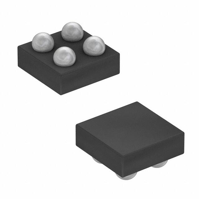
• 4 bump WCSP 0.8 mm x 0.8 mm with 0.4 mm pitch
package
• Material categorization: for definitions of compliance
please see www.vishay.com/doc?99912
SiP32451 features an output discharge for fast turn off.
SiP32451, SiP32452, and SiP32453 are available in compact
wafer level CSP package, WCSP4 0.8 mm x 0.8 mm with
0.4 mm pitch.
APPLICATIONS
• Battery operated devices
• Smart phones
• GPS and PMP
• Computer
• Medical and healthcare equipment
• Industrial and instrument
• Cellular phones and portable media players
• Game console
TYPICAL APPLICATION CIRCUIT
VIN
IN
OUT
VOUT
SiP32451, SiP32452, SiP32453
CIN
COUT
EN
GND
EN
GND
GND
Fig. 1 - SiP32451, SiP32452, and SiP32453 Typical Application Circuit
ORDERING INFORMATION
TEMPERATURE RANGE
-40 °C to +85 °C
PACKAGE
MARKING
PART NUMBER
WCSP4: 4 bumps
(2 x 2, 0.4 mm pitch,
208 μm bump height,
0.8 mm x 0.8 mm die size)
AA
SiP32451DB-T2-GE1
AB
SiP32452DB-T2-GE1
AC
SiP32453DB-T2-GE1
Note
• GE1 denotes halogen-free and RoHS-compliant
S20-0528-Rev. E, 06-Jul-2020
Document Number: 63315
1
For technical questions, contact: powerictechsupport@vishay.com
THIS DOCUMENT IS SUBJECT TO CHANGE WITHOUT NOTICE. THE PRODUCTS DESCRIBED HEREIN AND THIS DOCUMENT
ARE SUBJECT TO SPECIFIC DISCLAIMERS, SET FORTH AT www.vishay.com/doc?91000
�SiP32451, SiP32452, SiP32453
www.vishay.com
Vishay Siliconix
ABSOLUTE MAXIMUM RATINGS
PARAMETER
LIMIT
Supply input voltage (VIN)
UNIT
-0.3 to +2.75
Enable input voltage (VEN)
-0.3 to +2.75
Output voltage (VOUT)
-0.3 to +2.75
Maximum continuous switch current (Imax.)
V
1.2
Maximum pulsed current (IDM) VIN (pulsed at 1 ms, 10 % duty cycle)
A
2
ESD rating (HBM)
4000
V
Junction temperature (TJ)
-40 to +150
°C
Thermal resistance (JA) a
280
°C/W
Power dissipation (PD) a
196
mW
Notes
a. Device mounted with all leads and power pad soldered or welded to PC board
b. Derate 3.6 mW/°C above TA = 70 °C
Stresses beyond those listed under “Absolute Maximum Ratings” may cause permanent damage to the device. These are stress ratings only, and functional operation
of the device at these or any other conditions beyond those indicated in the operational sections of the specifications is not implied. Exposure to absolute maximum
rating/conditions for extended periods may affect device reliability.
RECOMMENDED OPERATING RANGE
PARAMETER
LIMIT
Input voltage range (VIN)
Operating junction temperature range
UNIT
0.9 to 2.5
V
-40 to +125
°C
SPECIFICATIONS
PARAMETER
SYMBOL
Operating voltage c
TEST CONDITIONS UNLESS SPECIFIED
VIN = 1 V, TA = -40 °C to +85 °C
(typical values are at TA = 25 °C)
TYP. b
MAX. a
0.9
-
2.5
-
10
15
VIN = 2.5 V, VEN = VIN, OUT = open
-
34
60
SiP32451
-
-
30
-
-
1
VIN
Quiescent current
IQ
LIMITS
VIN = 1.2 V, VEN = VIN, OUT = open
MIN. a
Off supply current
IQ(off)
Off switch current
IDS(off)
EN = GND, OUT = 0 V
-
-
30
IRB
VOUT = 2.5 V, VIN = 0.9 V, VEN = 0 V
-
0.001
10
Reverse blocking current
On-resistance
RDS(on)
On-resistance temp. coefficient
TCRDS
Output pull-down resistance
EN input low voltage
c
RPD
SiP32452, SiP32453
EN = GND, OUT = open
V
μA
VIN = 1 V, IL = 200 mA, TA = 25 °C
-
56
65
VIN = 1.2 V, IL = 200 mA, TA = 25 °C
-
55
65
VIN = 1.8 V, IL = 200 mA, TA = 25 °C
-
54
65
VIN = 2.5 V, IL = 200 mA, TA = 25 °C
-
54
65
-
3900
-
ppm/°C
-
425
550
VEN = 0 V, TA = 25 °C (SiP32451 only)
VIL
VIN = 1 V
-
-
0.1
EN input high voltage c
VIH
VIN = 2.5 V
1.5
-
-
EN input leakage
IEN
VIN = 2.5 V, VEN = 0 V
-
-
1
VIN = 2.5 V, VEN = 2.5 V
-
10
15
S20-0528-Rev. E, 06-Jul-2020
UNIT
m
V
μA
Document Number: 63315
2
For technical questions, contact: powerictechsupport@vishay.com
THIS DOCUMENT IS SUBJECT TO CHANGE WITHOUT NOTICE. THE PRODUCTS DESCRIBED HEREIN AND THIS DOCUMENT
ARE SUBJECT TO SPECIFIC DISCLAIMERS, SET FORTH AT www.vishay.com/doc?91000
�SiP32451, SiP32452, SiP32453
www.vishay.com
Vishay Siliconix
SPECIFICATIONS
PARAMETER
SYMBOL
Output turn-on delay time
Output turn-on rise time
TEST CONDITIONS UNLESS SPECIFIED
VIN = 1 V, TA = -40 °C to +85 °C
(typical values are at TA = 25 °C)
TYP. b
MAX. a
-
0.4
1
VIN = 2.5 V
-
0.05
1
VIN = 1.2 V
10
20
30
5
9.8
20
-
0.25
1
SiP32451, SiP32452
VIN = 2.5 V
-
0.15
1
SiP32453, VIN = 1.2 V
30
98
150
SiP32453, VIN = 2.5 V
30
86
150
VIN = 1.2 V
td(on)
tr
VIN = 2.5 V
SiP32451, SiP32452
VIN = 1.2 V
Output turn-off delay time
td(off)
LIMITS
RLOAD = 10 ,
CL = 0.1 μF, TA = 25 °C
MIN.
a
UNIT
μs
Notes
a. The algebraic convention whereby the most negative value is a minimum and the most positive a maximum
b. Typical values are for DESIGN AID ONLY, not guaranteed nor subject to production testing
c. For VIN outside this range consult typical EN threshold curve
PIN CONFIGURATION
Index-Bump A1
1
IN
A
B
A
EN
2
OUT
2
OUT
1
IN
W
A
B
B
GND
Backside
GND
EN
Bumpside
Fig. 2 - WCSP4 2 x 2 Package
PIN DESCRIPTION
PIN NUMBER
NAME
A1
IN
A2
OUT
B1
EN
B2
GND
S20-0528-Rev. E, 06-Jul-2020
FUNCTION
This pin is the n-channel MOSFET drain connection. Bypass to ground through a 4.7 μF capacitor
This pin is the n-channel MOSFET source connection. Bypass to ground through a 0.1 μF capacitor
Enable input
Ground connection
Document Number: 63315
3
For technical questions, contact: powerictechsupport@vishay.com
THIS DOCUMENT IS SUBJECT TO CHANGE WITHOUT NOTICE. THE PRODUCTS DESCRIBED HEREIN AND THIS DOCUMENT
ARE SUBJECT TO SPECIFIC DISCLAIMERS, SET FORTH AT www.vishay.com/doc?91000
�SiP32451, SiP32452, SiP32453
www.vishay.com
Vishay Siliconix
TYPICAL CHARACTERISTICS (internally regulated, 25 °C, unless otherwise noted)
45
1000
SiP32452 and SiP32453
100
IQ(OFF) - Off Supply Current (nA)
I Q - Quiescent Current (μA)
40
35
30
25
20
15
10
10
VIN = 2.5 V
1
0.1
0.01
VIN = 1 V
0.001
5
0
0.8
1.0
1.2
1.4
1.6
1.8 2.0
V IN (V)
2.2
2.4
2.6
2.8
0.0001
- 40
- 20
0
20
60
80
100
Fig. 6 - Off Supply Current vs. Temperature
1200
12
SiP32452 and SiP32453
SiP32451
1100
IQ(OFF) - Off Supply Current (nA)
10
8
6
4
2
1000
900
800
700
600
500
400
0.8
0
0.8
1.2
1.6
2.0
2.4
2.8
1.0
1.2
1.4
1.6
VIN (V)
1.8
2.0
2.2
2.4
2.6
2.8
VIN (V)
Fig. 7 - Off Supply Current vs. Input Voltage
Fig. 4 - Off Supply Current vs. Input Voltage
1000
50
45
900
IDS(off) - Off Switch Current (nA)
VIN = 2.5 V
IQ - Quiescent Current (μA)
40
Temperature (°C)
Fig. 3 - Quiescent Current vs. Input Voltage
IQ(OFF) - Off Supply Current (nA)
VIN = 1.2 V
40
35
30
25
20
15
VIN = 1.2 V
10
800
700
600
500
400
300
5
VIN = 1 V
0
- 40
- 20
0
20
40
60
Temperature (°C)
80
100
Fig. 5 - Quiescent Current vs. Temperature
S20-0528-Rev. E, 06-Jul-2020
200
0.8
1.2
1.6
2
2.4
2.8
VIN (V)
Fig. 8 - Off Switch Current vs. Input Voltage
Document Number: 63315
4
For technical questions, contact: powerictechsupport@vishay.com
THIS DOCUMENT IS SUBJECT TO CHANGE WITHOUT NOTICE. THE PRODUCTS DESCRIBED HEREIN AND THIS DOCUMENT
ARE SUBJECT TO SPECIFIC DISCLAIMERS, SET FORTH AT www.vishay.com/doc?91000
�SiP32451, SiP32452, SiP32453
www.vishay.com
Vishay Siliconix
TYPICAL CHARACTERISTICS (internally regulated, 25 °C, unless otherwise noted)
66
75
VIN = 1.2 V
70
62
60
RDS - On-Resistance (mΩ)
RDS - On-Resistance (mΩ)
64
IO = 1.2 A
58
IO = 0.5 A
56
54
50
0.8
1.2
1.6
2.0
65
60
55
50
45
IO = 0.2 A
52
IO = 200 mA
2.4
40
-40
2.8
-20
0
VIN (V)
Fig. 9 - RDS(on) vs. VIN
80
100
Fig. 12 - RDS(on) vs. Temperature
100 000
12
VIN = 2.5 V
SiP32451
10
IEN - EN Current (μA)
VIN = 2.5 V
10 000
IIQ(OFF) - Off Supply Current (nA)
20
40
60
Temperature (°C)
VIN = 1.2 V
1000
100
VIN = 1 V
8
6
4
10
2
1
-40
0
-20
0
20
40
60
80
100
0
0.5
1
1.5
Temperature (°C)
VEN (V)
Fig. 10 - Off Supply Current vs. Temperature
Fig. 13 - IEN vs. VEN
100 000
2
2.5
100
VOUT = 2.5 V
80
VIN = 1.2 V
1000
60
I IN (nA)
IDS(off) - Off Switch Current (nA)
VIN = 0.9 V
VIN = 2.5 V
10 000
100
40
VIN = 1 V
10
20
1
0
- 40
0
- 20
0
20
40
60
80
100
Temperature (°C)
Fig. 11 - Off Switch Current vs. Temperature
S20-0528-Rev. E, 06-Jul-2020
-40
-20
0
20
40
60
Temperature (°C)
80
100
Fig. 14 - Reverse Blocking Current vs. Temperature
Document Number: 63315
5
For technical questions, contact: powerictechsupport@vishay.com
THIS DOCUMENT IS SUBJECT TO CHANGE WITHOUT NOTICE. THE PRODUCTS DESCRIBED HEREIN AND THIS DOCUMENT
ARE SUBJECT TO SPECIFIC DISCLAIMERS, SET FORTH AT www.vishay.com/doc?91000
�SiP32451, SiP32452, SiP32453
www.vishay.com
Vishay Siliconix
TYPICAL CHARACTERISTICS (internally regulated, 25 °C, unless otherwise noted)
460
SiP32451 only
VOUT = VIN
435
RPD - Output Pulldown Resistance (Ω)
RPD - Output Pulldown Resistance (Ω)
440
430
425
420
415
SiP32451 only
VOUT = VIN = 2.5 V
450
440
430
420
410
400
410
0.8
1.0
1.2
1.4
1.6
1.8
2.0
2.2
2.4
2.6
-40
2.8
-20
VIN (V)
40
60
80
100
Temperature (°C)
2.0
0.100
VIN = 0.9 V
1.8
VIN = 2.5 V
CL = 0.1 μF
RL = 10 Ω
0.095
td(on) - Turn-On Delay Time (μs)
1.6
1.4
1.2
1.0
0.8
0.6
0.4
0.2
0.090
0.085
0.080
0.075
0.070
0.065
0.060
0.055
0
0.8
1
1.2
1.4
1.6
1.8
2
2.2
2.4
2.6
0.050
-40
2.8
-20
0
VOUT (V)
20
40
60
Temperature (°C)
80
100
Fig. 19 - Turn-On Delay Time vs. Temperature
Fig. 16 - Reverse Blocking Current vs. Output Voltage
1.6
0.30
SiP32451 and SiP32452
VIN = 2.5 V
CL = 0.1 μF
RL = 10 Ω
td(off) - Turn Off Delay Time (μs)
1.4
EN Threshold Voltage (V)
20
Fig. 18 - Output Pull-down Resistance vs. Temperature
Fig. 15 - Output Pull-down Resistance vs. Input Voltage
I IN (nA)
0
1.2
1.0
VIH
0.8
VIL
0.6
0.4
0.25
0.20
0.15
0.10
0.05
0.2
0.0
0.8 1.0
1.2
1.4
1.6
1.8 2.0
VIN (V)
2.2
2.4
2.6
2.8
Fig. 17 - EN Threshold Voltage vs. Input Voltage
S20-0528-Rev. E, 06-Jul-2020
0.00
-40
-20
0
20
40
Temperature (°C)
60
80
100
Fig. 20 - Turn-Off Delay Time vs. Temperature
Document Number: 63315
6
For technical questions, contact: powerictechsupport@vishay.com
THIS DOCUMENT IS SUBJECT TO CHANGE WITHOUT NOTICE. THE PRODUCTS DESCRIBED HEREIN AND THIS DOCUMENT
ARE SUBJECT TO SPECIFIC DISCLAIMERS, SET FORTH AT www.vishay.com/doc?91000
�SiP32451, SiP32452, SiP32453
www.vishay.com
Vishay Siliconix
TYPICAL CHARACTERISTICS (internally regulated, 25 °C, unless otherwise noted)
14
12
td(off) - Turn Off Delay Time (μs)
tr - Rise Switching Time (μs)
13
120
VIN = 2.5 V
CL = 0.1 μF
RL = 10 Ω
11
10
9
8
7
SiP32453
VIN = 2.5 V
CL = 0.1 μF
RL = 10 Ω
110
100
90
80
70
6
5
-40
-20
0
20
40
Temperature (°C)
60
80
100
Fig. 21 - Rise Time vs. Temperature
60
-40
-20
0
20
40
Temperature (°C)
60
80
100
Fig. 22 - Turn-Off Delay Time vs. Temperature
TYPICAL WAVEFORMS
Fig. 23 - Turn-On Time (VIN = 1.2 V)
Fig. 25 - SiP32453 Turn-Off Time (VIN = 1.2 V)
Fig. 24 - SiP32451 and SiP32452 Turn-Off Time (VIN = 1.2 V)
Fig. 26 - Turn-On Time (VIN = 2.5 V)
S20-0528-Rev. E, 06-Jul-2020
Document Number: 63315
7
For technical questions, contact: powerictechsupport@vishay.com
THIS DOCUMENT IS SUBJECT TO CHANGE WITHOUT NOTICE. THE PRODUCTS DESCRIBED HEREIN AND THIS DOCUMENT
ARE SUBJECT TO SPECIFIC DISCLAIMERS, SET FORTH AT www.vishay.com/doc?91000
�SiP32451, SiP32452, SiP32453
www.vishay.com
Vishay Siliconix
Fig. 27 - SiP32451 and SiP32452 Turn-Off Time (VIN = 2.5 V)
Fig. 28 - SiP32453 Turn-Off Time (VIN = 2.5 V)
BLOCK DIAGRAM
IN
EN
OUT
Control
Logic
Charge
Pump
GND
Fig. 29 - Functional Block Diagram
DETAILED DESCRIPTION
SiP32451, SiP32452, and SiP32453 are n-channel power
MOSFET designed as high side load switch. Once enable
the device charge pumps the gate of the power MOSFET to
a constant gate to source voltage for fast turn on time. The
mostly constant gate to source voltage keeps the on
resistance low through out the input voltage range. When
disable, the SiP32451 and SiP32452 pull the gate of the
output n-channel low right away for a fast turn off delay
while there is a build-in turn off delay for the SiP32453. The
SiP32451 especially features a output discharge circuit to
help discharge the output capacitor. The turn off delay for
the SiP32453 is guaranteed to be at least 30 μs. Because
the body of the output n-channel is always connected to
GND, it prevents the current from going back to the input in
case the output voltage is higher than the output.
APPLICATION INFORMATION
Input Capacitor
While a bypass capacitor on the input is not required,
a 4.7 μF or larger capacitor for CIN is recommended in
almost all applications. The bypass capacitor should be
placed as physically close as possible to the input pin to be
effective in minimizing transients on the input. Ceramic
capacitors are recommended over tantalum because of
S20-0528-Rev. E, 06-Jul-2020
their ability to withstand input current surges from low
impedance sources such as batteries in portable devices.
Output Capacitor
A 0.1 μF capacitor across VOUT and GND is recommended
to insure proper slew operation. There is inrush current
through the output MOSFET and the magnitude of the
inrush current depends on the output capacitor, the bigger
the COUT the higher the inrush current. There are no ESR or
capacitor type requirement.
Enable
The EN pin is compatible with CMOS logic voltage levels. It
requires at least 0.1 V or below to fully shut down the device
and 1.5 V or above to fully turn on the device.
Protection Against Reverse Voltage Condition
SiP32451, SiP32452, and SiP32453 can block the output
current from going to the input in case where the output
voltage is higher than the input voltage when the main
switch is off.
Thermal Considerations
These devices are designed to maintain a constant output
load current. Due to physical limitations of the layout and
assembly of the device the maximum switch current is 1.2 A
as stated in the Absolute Maximum Ratings table. However,
Document Number: 63315
8
For technical questions, contact: powerictechsupport@vishay.com
THIS DOCUMENT IS SUBJECT TO CHANGE WITHOUT NOTICE. THE PRODUCTS DESCRIBED HEREIN AND THIS DOCUMENT
ARE SUBJECT TO SPECIFIC DISCLAIMERS, SET FORTH AT www.vishay.com/doc?91000
�SiP32451, SiP32452, SiP32453
www.vishay.com
another limiting characteristic for the safe operating load
current is the thermal power dissipation of the package. To
obtain the highest power dissipation (and a thermal
resistance of 280 °C/W) the device should be connected to
a heat sink on the printed circuit board.
The maximum power dissipation in any application is
dependent on the maximum junction temperature,
TJ (max.) = 125 °C, the junction-to-ambient thermal
resistance, J-A = 280 °C/W, and the ambient temperature,
TA, which may be formulaically expressed as:
125 - T A
T J(max.) - T A
P (max.) = -------------------------------- = ---------------------- JA
280
It then follows that, assuming an ambient temperature of
70 °C, the maximum power dissipation will be limited to
about 196 mW.
So long as the load current is below the 1.2 A limit, the
maximum continuous switch current becomes a function
two things: the package power dissipation and the RDS(on) at
the ambient temperature.
As an example let us calculate the worst case maximum
load current at TA = 70 °C. The worst case RDS(on) at 25 °C is
S20-0528-Rev. E, 06-Jul-2020
Vishay Siliconix
65 m. The RDS(on) at 70 °C can be extrapolated from this
data using the following formula:
RDS(on) (at 70 °C) = RDS(on) (at 25 °C) x (1 + TC x T)
Where TC is 3900 ppm/°C. Continuing with the calculation
we have
RDS(on) (at 70 °C) = 65 m x (1 + 0.0039 x (70 °C - 25 °C))
= 76.4 m
The maximum current limit is then determined by
P (max.)
I LOAD(max.) --------------------R DS(on)
which in this case is 1.6 A. Under the stated input voltage
condition, if the 1.6 A current limit is exceeded the internal
die temperature will rise and eventually, possibly damage
the device.
To avoid possible permanent damage to the device and
keep a reasonable design margin, it is recommended to
operate the device maximum up to 1.2 A only as listed in the
Absolute Maximum Ratings table.
Document Number: 63315
9
For technical questions, contact: powerictechsupport@vishay.com
THIS DOCUMENT IS SUBJECT TO CHANGE WITHOUT NOTICE. THE PRODUCTS DESCRIBED HEREIN AND THIS DOCUMENT
ARE SUBJECT TO SPECIFIC DISCLAIMERS, SET FORTH AT www.vishay.com/doc?91000
�SiP32451, SiP32452, SiP32453
www.vishay.com
Vishay Siliconix
PRODUCT SUMMARY
Part number
SiP32451
SiP32452
SiP32453
Description
0.9 V to 2.5 V, 55 m,
bidirectional off isolation,
fast turn on / off, output
discharge
0.9 V to 2.5 V, 55 m,
bidirectional off isolation,
fast turn on / off
0.9 V to 2.5 V, 55 m,
bidirectional off isolation,
fast turn on and 98 μs turn
off delay
Single
Configuration
Single
Single
Slew rate time (μs)
20
20
20
On delay time (μs)
0.4
0.4
0.4
Input voltage min. (V)
0.9
0.9
0.9
Input voltage max. (V)
2.5
2.5
2.5
On-resistance at input voltage min. (m)
56
56
56
54
On-resistance at input voltage max. (m)
54
54
Quiescent current at input voltage min. (μA)
4
4
4
Quiescent current at input voltage max. (μA)
32
32
32
Output discharge (yes / no)
Yes
No
No
Reverse blocking (yes / no)
Yes
Yes
Yes
Continuous current (A)
Package type
Package size (W, L, H) (mm)
1.2
1.2
1.2
WCSP4
WCSP4
WCSP4
0.8 x 0.8 x 0.5
0.8 x 0.8 x 0.5
0.8 x 0.8 x 0.5
Status code
2
2
2
Product type
Slew rate
Slew rate
Slew rate
Applications
Computers, consumer,
industrial, healthcare,
networking, portable
Computers, consumer,
industrial, healthcare,
networking, portable
Computers, consumer,
industrial, healthcare,
networking, portable
Vishay Siliconix maintains worldwide manufacturing capability. Products may be manufactured at one of several qualified locations. Reliability data for Silicon
Technology and Package Reliability represent a composite of all qualified locations. For related documents such as package/tape drawings, part marking, and
reliability data, see www.vishay.com/ppg?63315
S20-0528-Rev. E, 06-Jul-2020
Document Number: 63315
10
For technical questions, contact: powerictechsupport@vishay.com
THIS DOCUMENT IS SUBJECT TO CHANGE WITHOUT NOTICE. THE PRODUCTS DESCRIBED HEREIN AND THIS DOCUMENT
ARE SUBJECT TO SPECIFIC DISCLAIMERS, SET FORTH AT www.vishay.com/doc?91000
�Package Information
www.vishay.com
Vishay Siliconix
WCSP4: 4 Bumps
(2 x 2, 0.4 mm pitch, 208 μm bump height, 0.8 mm x 0.8 mm die size)
Mark on backside of die
1
A
2
1
2
W
A
A
B
B
B
e
D
4 x Ø 0.15 to Ø 0.20
Solder mask dia. - Pad diameter + 0.1
0.4
e
4xØb
D
Pin 1 mark
A
0.4
Note 3
A1
Recommended Land Pattern
All dimensions in millimeters
Bump Note 2
DWG-No: 6004
Notes
(1) Laser mark on the backside surface of die
(2) Bumps are SAC396
(3) 0.05 max. coplanarity
DIM.
A
MILLIMETERS a
NOM.
MAX.
MIN.
NOM.
MAX.
0.515
0.530
0.545
0.0203
0.0209
0.0215
0.250
0.260
0.270
0.0098
0.800
0.0283
A1
b
0.208
e
D
INCHES
MIN.
0.0082
0.400
0.720
0.760
0.0102
0.0106
0.0157
0.0299
0.0315
Note
a. Use millimeters as the primary measurement
T19-0364-Rev. D, 07-Oct-2019
1
Document Number: 63459
THIS DOCUMENT IS SUBJECT TO CHANGE WITHOUT NOTICE. THE PRODUCTS DESCRIBED HEREIN AND THIS DOCUMENT
ARE SUBJECT TO SPECIFIC DISCLAIMERS, SET FORTH AT www.vishay.com/doc?91000
�Legal Disclaimer Notice
www.vishay.com
Vishay
Disclaimer
ALL PRODUCT, PRODUCT SPECIFICATIONS AND DATA ARE SUBJECT TO CHANGE WITHOUT NOTICE TO IMPROVE
RELIABILITY, FUNCTION OR DESIGN OR OTHERWISE.
Vishay Intertechnology, Inc., its affiliates, agents, and employees, and all persons acting on its or their behalf (collectively,
“Vishay”), disclaim any and all liability for any errors, inaccuracies or incompleteness contained in any datasheet or in any other
disclosure relating to any product.
Vishay makes no warranty, representation or guarantee regarding the suitability of the products for any particular purpose or
the continuing production of any product. To the maximum extent permitted by applicable law, Vishay disclaims (i) any and all
liability arising out of the application or use of any product, (ii) any and all liability, including without limitation special,
consequential or incidental damages, and (iii) any and all implied warranties, including warranties of fitness for particular
purpose, non-infringement and merchantability.
Statements regarding the suitability of products for certain types of applications are based on Vishay's knowledge of typical
requirements that are often placed on Vishay products in generic applications. Such statements are not binding statements
about the suitability of products for a particular application. It is the customer's responsibility to validate that a particular product
with the properties described in the product specification is suitable for use in a particular application. Parameters provided in
datasheets and / or specifications may vary in different applications and performance may vary over time. All operating
parameters, including typical parameters, must be validated for each customer application by the customer's technical experts.
Product specifications do not expand or otherwise modify Vishay's terms and conditions of purchase, including but not limited
to the warranty expressed therein.
Hyperlinks included in this datasheet may direct users to third-party websites. These links are provided as a convenience and
for informational purposes only. Inclusion of these hyperlinks does not constitute an endorsement or an approval by Vishay of
any of the products, services or opinions of the corporation, organization or individual associated with the third-party website.
Vishay disclaims any and all liability and bears no responsibility for the accuracy, legality or content of the third-party website
or for that of subsequent links.
Except as expressly indicated in writing, Vishay products are not designed for use in medical, life-saving, or life-sustaining
applications or for any other application in which the failure of the Vishay product could result in personal injury or death.
Customers using or selling Vishay products not expressly indicated for use in such applications do so at their own risk. Please
contact authorized Vishay personnel to obtain written terms and conditions regarding products designed for such applications.
No license, express or implied, by estoppel or otherwise, to any intellectual property rights is granted by this document or by
any conduct of Vishay. Product names and markings noted herein may be trademarks of their respective owners.
© 2022 VISHAY INTERTECHNOLOGY, INC. ALL RIGHTS RESERVED
Revision: 01-Jan-2022
1
Document Number: 91000
�