SiP41109, SiP41110
Vishay Siliconix
Half-Bridge N-Channel MOSFET Driver for DC/DC Conversion
DESCRIPTION
FEATURES
The SiP41109 and SiP41110 are high-speed half-bridge
MOSFET drivers for use in high frequency, high current,
multiphase dc-to-dc synchronous rectifier buck power
supplies. They are designed to operate at switching
frequencies up to 1 MHz. The high-side driver is
bootstrapped to allow driving N-channel MOSFETs.
•
•
•
•
•
•
•
•
•
They feature adaptive shoot-through protection to prevent
simultaneous conduction of the external MOSFETs. There
are two options available for the voltage of the high-side and
low-side drivers. In the SiP41109, the regulator supplies gate
drive voltage to the high-side driver and VCC supplies the
low-side driver. in the SiP41110, the regulator supplies the
high- and low-side gate drive voltage.
PWM with tri-state enable
12 V low-side gate drive (SiP41109)
8 V low-side gate drive (SiP41110)
Undervoltage lockout
Internal bootstrap diode
Switching frequency up to 1 MHz
30 ns max. propagation delay
Drive MOSFETs in 5 V to 48 V systems
Adaptive shoot-through protection
APPLICATIONS
•
•
•
•
•
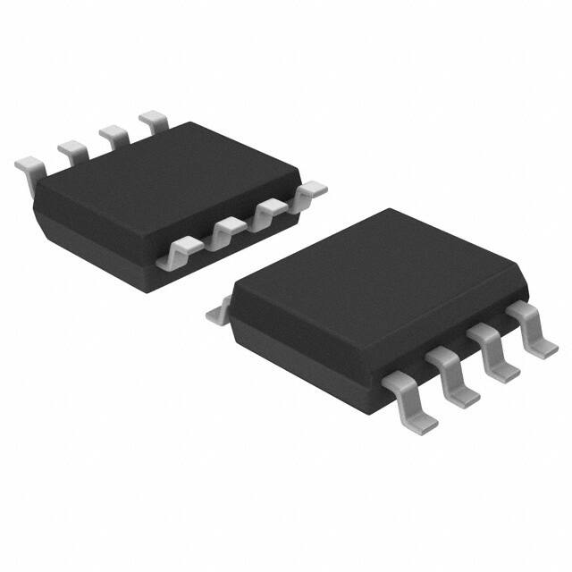
The SiP41109 and SiP41110 are assembled in a lead (Pb)free 8-pin SOIC package for operation over the industrial
operating range (- 40 °C to 85 °C).
Multi-phase DC/DC conversion
High current low voltage DC/DC converters
High frequency DC/DC converters
Mobile and desktop computer DC/DC converters
Core voltage supplies for PC micro-processors
TYPICAL APPLICATION CIRCUIT
+ 5 to 48 V
+ 12 V
PVcc
VCC
BOOT
UGATE
SiP41109/41110
PHASE
Controller
VOUT
PWM
(Tri-State)
LGATE
GND
GND
Document Number: 73023
S09-1453-Rev. B, 03-Aug-09
GND
www.vishay.com
1
�SiP41109, SiP41110
Vishay Siliconix
ABSOLUTE MAXIMUM RATINGS (all voltages referenced to GND = 0 V)
Parameter
Limit
VCC, PVCC
- 0.3 to 15
BOOT, PHASE
- 0.3 to 55
BOOT to PHASE
- 0.3 to 15
Storage Temperature
- 40 to 150
Operating Junction Temperature
Unit
V
°C
125
Power Dissipationa
SO-8
Thermal Impedance (ΘJA)b
770
mW
130
°C/W
Notes:
a. Device Mounted with all leads soldered or welded to PC board.
b. Derate 7.7 mW/°C.
Stresses beyond those listed under “Absolute Maximum Ratings” may cause permanent damage to the device. These are stress ratings only, and functional operation
of the device at these or any other conditions beyond those indicated in the operational sections of the specifications is not implied. Exposure to absolute maximum
rating conditions for extended periods may affect device reliability.
RECOMMENDED OPERATING RANGE (all voltages referenced to GND = 0 V)
Parameter
Limit
VCC
10.8 to 13.2
VLX
48
CBOOT
Unit
V
100 nF to 1 µF
BOOT to PHASE
Operating Temperature Range
8
V
- 40 to 85
°C
SPECIFICATIONSa
Parameter
Symbol
Test Conditions Unless Specified
VCC = 12 V, VBOOT - VPHASE = 8 V
TA = - 40 °C to 85 °C
Limits
Min.a
Typ.b
Max.a
Unit
13.2
V
Power Supplies
Supply Voltage
VDD
Quiescent Current
ICCQ
Supply Current
IDD
Tristate (Shutdown) Current
ICCT
10.8
PWM non-switching
fPWM = 100 kHz, CLOAD = 3 nF
5.6
SiP41109
12.5
SiP41110
11.0
PWM = open
850
9.5
mA
1200
µA
Reference Voltage
VBBM
Break-Before-Make
2.5
V
PWM Input
Input High
VIH
Input Low
VIL
IB
Bias Current
Tristate Threshold
Tristate Holdoff Timeoutc
High
VTSH
Low
VTSL
VDD
4.0
1.0
PWM 5 V or 0 V
± 600
± 1000
3.0
2.0
tTST
240
V
µA
V
ns
Bootstrap Diode
Forward Voltage
www.vishay.com
2
VF
IF = 40 mA, TA = 25 °C
0.70
0.85
1.0
V
Document Number: 73023
S09-1453-Rev. B, 03-Aug-09
�SiP41109, SiP41110
Vishay Siliconix
SPECIFICATIONSa
Parameter
MOSFET Drivers
High-Side Drive Currentc
Low-Side Drive Currentc
High-Side Driver Impedance
Low-Side Driver Impedance
High-Side Rise Time
High-Side Fall Time
High-Side Rise Time Bypass
High-Side Fall Time Bypass
High-Side Propagation Delayc
Low-Side Rise Time
Low-Side Fall Time
Low-Side Propagation Delay
Symbol
IPKH(source)
IPKH(sink)
IPKL(source)
IPKL(sink)
IPKL(source)
IPKL(sink)
RDH(source)
RDH(sink)
RDL(source)
RDL(sink)
RDL(source)
RDL(sink)
trH
tfH
Test Conditions Unless Specified
VCC = 12 V, VBOOT - VPHASE = 8 V
TA = - 40 °C to 85 °C
Limits
Min.
SiP41110
VPVCC = 12 V
SiP41109
VBOOT - VPHASE = 8 V, PHASE = GND
VPVCC = 8 V
SiP41110
VPVCC = 12 V
SiP41109
10 % - 90 %, VBOOT - VPHASE = 8 V, CLOAD = 3 nF
10 % - 90 %, VBOOT - VPHASE = 12 V, CLOAD = 3 nF
td(off)H
td(on)H
trL
tfL
td(off)L
td(on)L
See Timing Waveforms
10 % to 90 %, VBOOT - VPHASE = 8 V
CLOAD = 3 nF
10 % to 90 %, VBOOT - VPHASE = 12 V
CLOAD = 3 nF
10 % to 90 %, VBOOT - VPHASE = 8 V
CLOAD = 3 nF
10 % to 90 %, VBOOT - VPHASE = 12 V
CLOAD = 3 nF
Typ.b
0.8
1.0
0.9
1.2
1.4
1.8
2.3
1.9
2.9
1.3
2.4
1.2
45
35
45
35
15
15
VBOOT - VPHASE = 8 V
VPVCC = 8 V
a
SiP41110
40
SiP41109
40
SiP41110
30
SiP41109
30
Max.a
Unit
A
4.2
3.5
5.2
2.4
4.3
2.2
Ω
ns
15
15
See Timing Waveforms
PHASE Timer
PHASE Falling Timeoutc
PVCC Regulator
Output Voltage
Output Current
Current Limit
Line Regulation
Load Regulation
PVCC Regulator UVLO
PVCC Rising
PVCC Falling
Hysteresis
High-Side Undervoltage Lockout
Threshold
VCC Undervoltage Lockout
Threshold
Power on Reset Time
Thermal Shutdown
Temperature
Hysteresis
tPHASE
PVCC
IPVCC
ILIM
LNR
LDR
380
7.6
VDRV = 0 V
VCC = 10.8 V to 13.2 V
5 mA to 80 mA
8
80
200
0.05
0.1
8.4
100
280
0.5
1.0
100
6.7
6.4
300
7.2
6.9
500
mV
2.5
3.35
4.0
V
5.0
5.3
2.5
5.6
V
ms
120
VUVLO2
Hyst
VUVHS
Rising or falling
VUVLO1
POR
TSD
TH
Temperature rising
Temperature ralling
ns
165
25
V
mA
%/V
%
V
°C
Notes:
a. The algebraic convention whereby the most negative value is a minimum and the most positive a maximum.
b. Typical values are for DESIGN AID ONLY, not guaranteed nor subject to production testing and are measured at VCC = 12 V unless otherwise
noted.
Document Number: 73023
S09-1453-Rev. B, 03-Aug-09
www.vishay.com
3
�SiP41109, SiP41110
Vishay Siliconix
TIMING WAVEFORMS
PWM
50 %
50 %
90 %
UGate
90 %
10 %
10 %
tfH
trH
90 %
90%
LGate
10 %
trL
td(off)H
10 %
tfL
td(off)L
td(on)H
td(on)L
Phase
2.5 V
PIN CONFIGURATION AND TRUTH TABLE
TRUTH TABLE
SO-8
UGATE
1
BOOT
2
SiP41109
PWM
3
SiP41110
GND
4
8
PHASE
7
PVCC
6
VCC
5
LGATE
PWM
UGATE
LGATE
L
L
H
L
H
L
Tri-State
L
L
ORDERING INFORMATION
Part Number
SiP41109DY-T1-E3
SiP41110DY-T1-E3
Top View
Eval Kit
SiP41109DB
SiP41110DB
Temperature Range
- 40 °C to 85 °C
Marking
41109
41110
Temperature Range
- 40 °C to 85 °C
PIN DESCRIPTION
Pin Number
Name
1
UGATE
8 V high-side MOSFET gate drive
Function
Bootstrap supply for high-side driver. The bootstap capacitor is connected between BOOT and PHASE.
2
BOOT
3
PWM
Input signal for the MOSFET drivers and tri-state enable
4
GND
Ground
5
LGATE
6
VCC
7
PVCC
8
PHASE
www.vishay.com
4
Synchronous or low-side MOSFET gate drive
12 V supply. Connect a bypass capacitor ≥ 1 µF from here to ground
8 V voltage regulator Output. Connect a bypass capacitor ≥ 1 µF from here to ground
Connection to source of high-side MOSFET, drain of the low-side MOSFET, and the inductor
Document Number: 73023
S09-1453-Rev. B, 03-Aug-09
�SiP41109, SiP41110
Vishay Siliconix
FUNCTIONAL BLOCK DIAGRAM
PVCC
+ 8 V Linear
Regulator
VCC
BOOT
UGATE
UVLO
OTP
UVLO
Linear
Regulator
+5V
PHASE
Tri-State
Detect
+
PWM
VBBM
(2.5 V)
VDRL
LGATE
GND
SiP41109 - VDRL = VCC (12 V)
SiP41110 - VDRL = PVCC (8 V)
Figure 1.
DETAILED OPERATION
PWM/Tri-State Enable
High-Side Driver
The PWM pin controls the switching of the external
MOSFETs. The driver logic operates in a noninverting
configuration. The PWM input stage should be driven by a
signal with fast transition times, like those provided by a
PWM controller or logic gate, (< 200 ns). The PWM input
functions as a logic input and is not intended for applications
where a slow changing input voltage is used to generate a
switching output when the input switching threshold voltage
is reached.
The high-side driver is isolated from the substrate to create a
floating high-side driver so that an N-channel MOSFET can
be used for the high-side switch. The high-side driver voltage
is supplied by PVCC. The voltage is maintained by a floating
bootstrap capacitor, which is continually recharged by the
switching action of the output. During shutdown UGATE is
held low.
Shutdown
The SiP41109/41110 enters shutdown mode when the
signal driving PWM enters the tri-state window for more than
240 ns. The shutdown state is removed when the PWM
signal moves outside the tri-state window. If the PWM is left
open, the pin is held to 2.5 V by an internal voltage divider,
thus forcing the tri-state condition.
Low-Side Driver
In the SiP41109, the low-side driver voltage is supplied by
VCC. In the SiP41110, the low-side driver voltage is supplied
by PVCC. During shutdown, LGATE is held low.
Gate Drive Voltage (PVCC) Regulator
An integrated 80 mA, 8 V regulator supplies voltage to the
PVCC pin and it current limits at 200 mA typical when the
output is shorted to ground. A capacitor (1 µF minimum)
must be connected to the PVCC pin to stabilize the regulator
output. The voltage on PVCC is supplied to the integrated
bootstrap diode. PVCC is used to recharge the bootstrap
capacitor and powers the SiP41110 low-side driver. PVCC
pin can be externally connected to VCC to bypass the 8 V
regulator and increase high-side gate drive to 12 V. If the
PVCC pin is connected to VCC the system voltage should not
exceed 43 V.
Bootstrap Circuit
The internal bootstrap diode and an external bootstrap
capacitor supply voltage to the BOOT pin. An integrated
bootstrap diode replaces the external diode normally needed
Document Number: 73023
S09-1453-Rev. B, 03-Aug-09
www.vishay.com
5
�SiP41109, SiP41110
Vishay Siliconix
for the bootstrap circuit; only a capacitor is necessary to
complete the bootstrap circuit. The bootstrap capacitor is
sized according to
2.5 V the high-side driver is enabled and UGATE will go high
after an internal propagation delay. If PHASE does not drop
below 2.5 V within 380 ns after UGATE goes low, LGATE is
forced high until the next PWM transition.
CBOOT = (QGATE/(ΔVBOOT - VPHASE)) x 10
where QGATE is the gate charge needed to turn on the highside MOSFET and ΔVBOOT - PHASE is the amount of droop
allowed in the bootstrapped supply voltage when the highside MOSFET is driven high. The bootstrap capacitor value
is typically 0.1 µF to 1 µF. The bootstrap capacitor voltage
rating must be greater than VCC + 12 V to withstand transient
spikes and ringing.
Shoot-Through Protection
The external MOSFETs are prevented from conducting at
the same time during transitions. Break-before-make circuits
monitor the voltages on the PHASE pin and the LGATE pin
and control the switching as follows: When the signal on
PWM goes low, UGATE will go low after an internal
propagation delay. After the voltage on PHASE falls below
2.5 V by the inductor action, the low-side driver is enabled
and LGATE goes high after some delay. When the signal on
PWM goes high, LGATE will go low after an internal
propagation delay. After the voltage on LGATE drops below
VCC Bypass Capacitor
MOSFET drivers draw large peak currents from the supplies
when they switch. A local bypass capacitor is required to
supply this current and reduce power supply noise. Connect
a 1 µF ceramic capacitor as close as practical between the
VCC and GND pins.
Undervoltage Lockout
Undervoltage lockout prevents control of the circuit until the
supply voltages reach valid operating levels. The UVLO
circuit forces LGATE and UGATE to low when VCC is below
its specified voltage. A separate UVLO forces UGATE low
when the voltage between BOOT and PHASE is below the
specified voltage.
Thermal Protection
If the die temperature rises above 165 °C, the thermal
protection disables the drivers. The drivers are re-enabled
after the die temperature has decreased below 140 °C.
TYPICAL CHARACTERISTICS
100
105
90
VCC = 12 V
85
80
75
70
65
1 MHz
55
ICC (mA)
ICC (mA)
95
500 kHz
VCC = 12 V
60
50
1 MHz
500 kHz
40
45
35
30
200 kHz
25
20
15
10
200 kHz
0
5
0
1
2
3
4
CLOAD (nF)
ICC vs. CLOAD vs. Frequency (SiP41109)
www.vishay.com
6
5
0
1
2
3
4
5
CLOAD (nF)
ICC vs. CLOAD vs. Frequency (SiP41110)
Document Number: 73023
S09-1453-Rev. B, 03-Aug-09
�SiP41109, SiP41110
Vishay Siliconix
TYPICAL WAVEFORMS
PWM
5 V/div
PWM
5 V/div
UGate
20 V/div
UGate
20 V/div
LGate
10 V/div
LGate
10 V/div
VPHASE
10 V/div
40 ns/div
Figure 2. PWM Signal vs. HS Gate, LS Gate
and PHASE (Rising)
VPHASE
10 V/div
40 ns/div
Figure 3. PWM Signal vs. HS Gate, LS Gate
and PHASE (Falling)
Vishay Siliconix maintains worldwide manufacturing capability. Products may be manufactured at one of several qualified locations. Reliability data for Silicon
Technology and Package Reliability represent a composite of all qualified locations. For related documents such as package/tape drawings, part marking, and
reliability data, see www.vishay.com/ppg?73023.
Document Number: 73023
S09-1453-Rev. B, 03-Aug-09
www.vishay.com
7
�Legal Disclaimer Notice
Vishay
Disclaimer
ALL PRODUCT, PRODUCT SPECIFICATIONS AND DATA ARE SUBJECT TO CHANGE WITHOUT NOTICE TO IMPROVE
RELIABILITY, FUNCTION OR DESIGN OR OTHERWISE.
Vishay Intertechnology, Inc., its affiliates, agents, and employees, and all persons acting on its or their behalf (collectively,
“Vishay”), disclaim any and all liability for any errors, inaccuracies or incompleteness contained in any datasheet or in any other
disclosure relating to any product.
Vishay makes no warranty, representation or guarantee regarding the suitability of the products for any particular purpose or
the continuing production of any product. To the maximum extent permitted by applicable law, Vishay disclaims (i) any and all
liability arising out of the application or use of any product, (ii) any and all liability, including without limitation special,
consequential or incidental damages, and (iii) any and all implied warranties, including warranties of fitness for particular
purpose, non-infringement and merchantability.
Statements regarding the suitability of products for certain types of applications are based on Vishay’s knowledge of typical
requirements that are often placed on Vishay products in generic applications. Such statements are not binding statements
about the suitability of products for a particular application. It is the customer’s responsibility to validate that a particular
product with the properties described in the product specification is suitable for use in a particular application. Parameters
provided in datasheets and/or specifications may vary in different applications and performance may vary over time. All
operating parameters, including typical parameters, must be validated for each customer application by the customer’s
technical experts. Product specifications do not expand or otherwise modify Vishay’s terms and conditions of purchase,
including but not limited to the warranty expressed therein.
Except as expressly indicated in writing, Vishay products are not designed for use in medical, life-saving, or life-sustaining
applications or for any other application in which the failure of the Vishay product could result in personal injury or death.
Customers using or selling Vishay products not expressly indicated for use in such applications do so at their own risk and agree
to fully indemnify and hold Vishay and its distributors harmless from and against any and all claims, liabilities, expenses and
damages arising or resulting in connection with such use or sale, including attorneys fees, even if such claim alleges that Vishay
or its distributor was negligent regarding the design or manufacture of the part. Please contact authorized Vishay personnel to
obtain written terms and conditions regarding products designed for such applications.
No license, express or implied, by estoppel or otherwise, to any intellectual property rights is granted by this document or by
any conduct of Vishay. Product names and markings noted herein may be trademarks of their respective owners.
Document Number: 91000
Revision: 11-Mar-11
www.vishay.com
1
�