SiSS28DN
www.vishay.com
Vishay Siliconix
N-Channel 25 V (D-S) MOSFET
FEATURES
PRODUCT SUMMARY
VDS (V)
25
RDS(on) () (MAX.)
ID (A) a, g
0.00152 at VGS = 10 V
60
0.00224 at VGS = 4.5 V
60
Qg (TYP.)
21.8 nC
• TrenchFET® Gen IV power MOSFET
• Optimized Qg, Qgd, and Qgd/Qgs ratio
reduces switching related power loss
• 100 % Rg and UIS tested
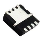
PowerPAK® 1212-8S
D
D
D 6 7
5
• Material categorization: for definitions of compliance
please see www.vishay.com/doc?99912
D
8
APPLICATIONS
D
• Synchronous rectification
• High power density DC/DC
3.
3
m
m
1
m
3m
3.
Top View
4
G
Bottom View
2
S
3
S
1
S
• VRMs and embedded DC/DC
G
• Synchronous buck converter
• Load switching
• Battery management
S
Ordering Information:
SiSS28DN-T1-GE3 (lead (Pb)-free and halogen-free)
N-Channel MOSFET
ABSOLUTE MAXIMUM RATINGS (TA = 25 °C, unless otherwise noted)
PARAMETER
SYMBOL
LIMIT
Drain-Source Voltage
VDS
25
Gate-Source Voltage
VGS
+16, -12
TC = 70 °C
TA = 25 °C
60 g
ID
41.8 b, c
33.1 b, c
TA = 70 °C
Pulsed Drain Current (t = 100 μs)
Continuous Source-Drain Diode Current
Single Pulse Avalanche Current
Single Pulse Avalanche Energy
IDM
TC = 25 °C
TA = 25 °C
L = 0.1 mH
TC = 70 °C
TA = 25 °C
41.8
IS
4.3 b, c
IAS
30
EAS
45
mJ
57
36
PD
W
4.8 b, c
3 b, c
TA = 70 °C
Operating Junction and Storage Temperature Range
A
150
TC = 25 °C
Maximum Power Dissipation
V
60 g
TC = 25 °C
Continuous Drain Current (TJ = 150 °C)
UNIT
TJ, Tstg
-55 to +150
Soldering Recommendations (Peak temperature) d, e
°C
260
THERMAL RESISTANCE RATINGS
PARAMETER
SYMBOL
TYPICAL
MAXIMUM
Maximum Junction-to-Ambient b, f
t 10 s
RthJA
21
26
Maximum Junction-to-Case (Drain)
Steady state
RthJC
1.7
2.2
UNIT
°C/W
Notes
a. Based on TC = 25 °C.
b. Surface mounted on 1" x 1" FR4 board.
c. t = 10 s.
d. See solder profile (www.vishay.com/doc?73257). The PowerPAK 1212-8S is a leadless package. The end of the lead terminal is exposed
copper (not plated) as a result of the singulation process in manufacturing. A solder fillet at the exposed copper tip cannot be guaranteed
and is not required to ensure adequate bottom side solder interconnection.
e. Rework conditions: manual soldering with a soldering iron is not recommended for leadless components.
f. Maximum under steady state conditions is 70 °C/W.
g. Package limited.
S16-1282-Rev. A, 27-Jun-16
Document Number: 76552
1
For technical questions, contact: pmostechsupport@vishay.com
THIS DOCUMENT IS SUBJECT TO CHANGE WITHOUT NOTICE. THE PRODUCTS DESCRIBED HEREIN AND THIS DOCUMENT
ARE SUBJECT TO SPECIFIC DISCLAIMERS, SET FORTH AT www.vishay.com/doc?91000
�SiSS28DN
www.vishay.com
Vishay Siliconix
SPECIFICATIONS (TJ = 25 °C, unless otherwise noted)
PARAMETER
SYMBOL
TEST CONDITIONS
MIN.
TYP.
MAX.
UNIT
V
Static
VDS
VGS = 0 V, ID = 250 μA
25
-
-
VDS/TJ
ID = 10 mA
-
19
-
VGS(th) Temperature Coefficient
VGS(th)/TJ
ID = 250 μA
-
-4.2
-
Gate-Source Threshold Voltage
Drain-Source Breakdown Voltage
VDS Temperature Coefficient
mV/°C
VGS(th)
VDS = VGS, ID = 250 μA
1
-
2
V
Gate-Source Leakage
IGSS
VDS = 0 V, VGS = +16 V, -12 V
-
-
± 100
nA
Zero Gate Voltage Drain Current
IDSS
VDS = 25 V, VGS = 0 V
-
-
1
V= 25 V, VDS GS = 0 V, TJ = 55 °C
-
-
10
On-State Drain Current a
ID(on)
VDS 5 V, VGS = 10 V
30
-
-
VGS = 10 V, ID = 15 A
-
0.00115 0.00152
VGS = 4.5 V, ID = 10 A
-
0.00160 0.00224
VDS = 10 V, ID = 15 A
-
Drain-Source On-State Resistance a
Forward Transconductance a
Dynamic
RDS(on)
gfs
95
-
μA
A
S
b
Input Capacitance
Ciss
-
3640
-
Output Capacitance
Coss
-
1155
-
Reverse Transfer Capacitance
Crss
-
200
-
VDS = 10 V, VGS = 0 V, f = 1 MHz
Crss/Ciss Ratio
V = 10 V, VGS = 10 V, ID = 10 A
-
0.043
0.085
-
48.1
75
-
21.8
35
-
8.6
-
-
3.4
-
Total Gate Charge
Qg
Gate-Source Charge
Qgs
Gate-Drain Charge
Qgd
Output Charge
Qoss
VDS = 10 V, VGS = 0 V
-
17.5
-
Rg
f = 1 MHz
0.2
0.7
1.4
-
11
22
-
18
36
-
30
60
Gate Resistance
Turn-On Delay Time
Rise Time
Turn-Off Delay Time
Fall Time
Turn-On Delay Time
Rise Time
Turn-Off Delay Time
Fall Time
VDS = 10 V, VGS = 4.5 V, ID = 10 A
td(on)
tr
td(off)
VDD = 10 V, RL = 1
ID 10 A, VGEN = 10 V, Rg = 1
tf
-
8
16
td(on)
-
23
46
-
27
54
tr
td(off)
VDD = 10 V, RL = 1
ID 10 A, VGEN = 4.5 V, Rg = 1
tf
-
28
56
-
10
20
-
-
48.1
-
-
150
pF
nC
ns
Drain-Source Body Diode Characteristics
Continuous Source-Drain Diode Current
IS
Pulse Diode Forward Current (t = 100 μs)
ISM
Body Diode Voltage
VSD
Body Diode Reverse Recovery Time
trr
Body Diode Reverse Recovery Charge
Qrr
Reverse Recovery Fall Time
ta
Reverse Recovery Rise Time
tb
TC = 25 °C
IS = 5 A
IF = 10 A, dI/dt = 100 A/μs,
TJ = 25 °C
A
-
0.73
1.1
V
-
36
72
ns
-
29
58
nC
-
16
-
-
20
-
ns
Notes
a. Pulse test; pulse width 300 μs, duty cycle 2 %.
b. Guaranteed by design, not subject to production testing.
Stresses beyond those listed under “Absolute Maximum Ratings” may cause permanent damage to the device. These are stress ratings only, and functional operation
of the device at these or any other conditions beyond those indicated in the operational sections of the specifications is not implied. Exposure to absolute maximum
rating conditions for extended periods may affect device reliability.
S16-1282-Rev. A, 27-Jun-16
Document Number: 76552
2
For technical questions, contact: pmostechsupport@vishay.com
THIS DOCUMENT IS SUBJECT TO CHANGE WITHOUT NOTICE. THE PRODUCTS DESCRIBED HEREIN AND THIS DOCUMENT
ARE SUBJECT TO SPECIFIC DISCLAIMERS, SET FORTH AT www.vishay.com/doc?91000
�SiSS28DN
www.vishay.com
Vishay Siliconix
TYPICAL CHARACTERISTICS (25 °C, unless otherwise noted)
Axis Title
Axis Title
150
150
10000
10000
VGS = 10 V thru 4 V
60
100
30
1000
90
1st line
2nd line
1000
90
2nd line
ID - Drain Current (A)
120
VGS = 3 V
1st line
2nd line
2nd line
ID - Drain Current (A)
120
TC = 25 °C
60
100
30
TC = 125 °C
TC = -55 °C
VGS = 2 V
0
0
10
0
0.4
0.8
1.2
1.6
2
10
0
1
2
VGS - Gate-to-Source Voltage (V)
2nd line
Output Characteristics
Transfer Characteristics
4500
10000
10000
Ciss
3600
1000
1st line
2nd line
0.0016
0.0014
100
VGS = 10 V
2nd line
C - Capacitance (pF)
VGS = 4.5 V
0.0012
1000
2700
1st line
2nd line
0.0018
5
Axis Title
Axis Title
1800
Coss
100
900
Crss
0.0010
0
10
0
20
40
60
80
10
0
100
5
10
20
ID - Drain Current (A)
2nd line
VDS - Drain-to-Source Voltage (V)
2nd line
On-Resistance vs. Drain Current
Capacitance
1.7
ID = 10 A
8
1000
1st line
2nd line
6
4
100
VDS = 5 V, 10 V, 15 V
2
0
10
20
30
40
50
2nd line
RDS(on) - On-Resistance (Normalized)
10000
10
25
Axis Title
Axis Title
10
0
15
10000
ID = 10 A
1.5
VGS = 10 V
1000
1.3
VGS = 4.5 V
1.1
100
0.9
0.7
10
-50
-25
0
25
50
75
100 125 150
Qg - Total Gate Charge (nC)
2nd line
TJ - Junction Temperature (°C)
2nd line
Gate Charge
On-Resistance vs. Junction Temperature
S16-1282-Rev. A, 27-Jun-16
1st line
2nd line
2nd line
RDS(on) - On-Resistance (Ω)
4
VDS - Drain-to-Source Voltage (V)
2nd line
0.0020
2nd line
VGS - Gate-to-Source Voltage (V)
3
Document Number: 76552
3
For technical questions, contact: pmostechsupport@vishay.com
THIS DOCUMENT IS SUBJECT TO CHANGE WITHOUT NOTICE. THE PRODUCTS DESCRIBED HEREIN AND THIS DOCUMENT
ARE SUBJECT TO SPECIFIC DISCLAIMERS, SET FORTH AT www.vishay.com/doc?91000
�SiSS28DN
www.vishay.com
Vishay Siliconix
TYPICAL CHARACTERISTICS (25 °C, unless otherwise noted)
Axis Title
Axis Title
100
0.010
10000
10000
1000
1
TJ = 25 °C
1st line
2nd line
2nd line
IS - Source Current (A)
TJ = 150 °C
0.1
100
0.01
0.008
1000
0.006
1st line
2nd line
2nd line
RDS(on) - On-Resistance (Ω)
ID = 10 A
10
0.004
TJ = 125 °C
100
0.002
TJ = 25 °C
0.001
0
10
0
0.2
0.4
0.6
0.8
1.0
1.2
10
0
2
4
8
10
VSD - Source-to-Drain Voltage (V)
2nd line
VGS - Gate-to-Source Voltage (V)
2nd line
Source-Drain Diode Forward Voltage
On-Resistance vs. Gate-to-Source Voltage
Axis Title
Axis Title
10000
0.4
10000
120
0.2
100
1000
-0.4
60
100
ID = 250 μA
1st line
2nd line
ID = 5 mA
-0.2
1000
80
2nd line
Power (W)
0
1st line
2nd line
2nd line
VGS(th) - Variance (V)
6
40
-0.6
100
20
-0.8
0
0.001
10
-50
-25
0
25
50
75
100 125 150
10
0.01
0.1
1
10
TJ - Temperature (°C)
2nd line
Time (s)
2nd line
Threshold Voltage
Single Pulse Power, Junction-to-Ambient
Axis Title
1000
10000
IDM limited
ID limited
100 μs 1000
10
1st line
2nd line
2nd line
ID - Drain Current (A)
100
1 ms
Limited by RDS(on) (1)
10 ms
1
100 ms 100
1s
10 s
0.1
TA = 25 °C
Single pulse
0.01
0.01
(1)
0.1
DC
BVDSS limited
1
10
10
100
VDS - Drain-to-Source Voltage (V)
VGS > minimum VGS at which RDS(on) is specified
Safe Operating Area
S16-1282-Rev. A, 27-Jun-16
Document Number: 76552
4
For technical questions, contact: pmostechsupport@vishay.com
THIS DOCUMENT IS SUBJECT TO CHANGE WITHOUT NOTICE. THE PRODUCTS DESCRIBED HEREIN AND THIS DOCUMENT
ARE SUBJECT TO SPECIFIC DISCLAIMERS, SET FORTH AT www.vishay.com/doc?91000
�SiSS28DN
www.vishay.com
Vishay Siliconix
TYPICAL CHARACTERISTICS (25 °C, unless otherwise noted)
Axis Title
180
10000
1000
108
1st line
2nd line
2nd line
ID - Drain Current (A)
144
Package Limited
72
100
36
0
10
0
25
50
75
100
125
150
TC - Case Temperature (°C)
2nd line
Current Derating a
Axis Title
Axis Title
70
10000
2.5
56
10000
2.0
1.5
1st line
2nd line
28
2nd line
Power (W)
1000
1st line
2nd line
2nd line
Power (W)
1000
42
1.0
100
14
100
0.5
0
10
0
25
50
75
100
125
150
0
10
0
25
50
75
100
125
TC - Case Temperature (°C)
2nd line
TA - Ambient Temperature (°C)
2nd line
Power, Junction-to-Case
Power, Junction-to-Ambient
150
Note
a. The power dissipation PD is based on TJ (max.) = 150 °C, using junction-to-case thermal resistance, and is more useful in settling the upper
dissipation limit for cases where additional heatsinking is used. It is used to determine the current rating, when this rating falls below the
package limit.
S16-1282-Rev. A, 27-Jun-16
Document Number: 76552
5
For technical questions, contact: pmostechsupport@vishay.com
THIS DOCUMENT IS SUBJECT TO CHANGE WITHOUT NOTICE. THE PRODUCTS DESCRIBED HEREIN AND THIS DOCUMENT
ARE SUBJECT TO SPECIFIC DISCLAIMERS, SET FORTH AT www.vishay.com/doc?91000
�SiSS28DN
www.vishay.com
Vishay Siliconix
TYPICAL CHARACTERISTICS (25 °C, unless otherwise noted)
Axis Title
10000
Duty cycle = 0.5
0.1
0.2
Notes:
0.1
PDM
1000
1st line
2nd line
Normalized Effective Transient
Thermal Impedance
1
t1
0.05
t2
t
1. Duty cycle, D = t1
2
2. Per unit base = RthJA = 70 °C/W
0.02
3. TJM - TA = PDMZthJA
Single pulse
100
(t)
4. Surface mounted
0.01
0.0001
0.001
0.01
0.1
1
10
100
10
1000
Square Wave Pulse Duration (s)
2nd line
Normalized Thermal Transient Impedance, Junction-to-Ambient
Axis Title
10000
Duty cycle = 0.5
1000
0.2
1st line
2nd line
Normalized Effective Transient
Thermal Impedance
1
0.1
0.05
100
0.02
Single pulse
0.1
0.0001
10
0.001
0.01
0.1
1
10
Square Wave Pulse Duration (s)
2nd line
Normalized Thermal Transient Impedance, Junction-to-Case
Vishay Siliconix maintains worldwide manufacturing capability. Products may be manufactured at one of several qualified locations. Reliability data for Silicon
Technology and Package Reliability represent a composite of all qualified locations. For related documents such as package/tape drawings, part marking, and
reliability data, see www.vishay.com/ppg?76552.
S16-1282-Rev. A, 27-Jun-16
Document Number: 76552
6
For technical questions, contact: pmostechsupport@vishay.com
THIS DOCUMENT IS SUBJECT TO CHANGE WITHOUT NOTICE. THE PRODUCTS DESCRIBED HEREIN AND THIS DOCUMENT
ARE SUBJECT TO SPECIFIC DISCLAIMERS, SET FORTH AT www.vishay.com/doc?91000
�Package Information
www.vishay.com
Vishay Siliconix
Case Outline for PowerPAK® 1212-8S
A
0.10 C
2x
D
8
7
Z
6
5
D1
5
6
b
4
3
7
8
2
1
K1
E1
E
K
B
L
0.10 C
1
2x
2
3
4
Pin 1 dot
e
0.10 M C A B
0.05 M C
0.10 C
C
A
A3
0.08 C
A1
A
MIN.
0.67
MILLIMETERS
NOM.
0.75
MAX.
0.83
MIN.
0.026
INCHES
NOM.
0.030
MAX.
0.033
A1
0.00
-
0.05
0.000
-
0.002
DIM.
A3
0.20 ref.
0.008 ref
b
0.25
0.30
0.35
0.010
0.012
D
3.20
3.30
3.40
0.126
0.130
0.134
D1
2.15
2.25
2.35
0.085
0.089
0.093
E
3.20
3.30
3.40
0.126
0.130
0.134
E1
1.60
1.70
1.80
0.063
0.067
0.071
e
0.65 bsc.
0.026 bsc.
K
0.76 ref.
0.030 ref.
K1
L
0.41 ref.
0.33
Z
0.43
0.525 ref.
0.014
0.016 ref.
0.53
0.013
0.017
0.021
0.021 ref.
ECN: C20-0862-Rev. B, 20-Jul-2020
DWG: 6008
Revision: 20-Jul-2020
Document Number: 63919
1
For technical questions, contact: pmostechsupport@vishay.com
THIS DOCUMENT IS SUBJECT TO CHANGE WITHOUT NOTICE. THE PRODUCTS DESCRIBED HEREIN AND THIS DOCUMENT
ARE SUBJECT TO SPECIFIC DISCLAIMERS, SET FORTH AT www.vishay.com/doc?91000
�Application Note 826
Vishay Siliconix
RECOMMENDED MINIMUM PADS FOR PowerPAK® 1212-8 Single
0.152
(3.860)
0.039
0.068
(0.990)
(1.725)
0.010
(0.255)
(2.390)
0.094
0.088
(2.235)
0.016
(0.405)
0.026
(0.660)
0.025
0.030
(0.635)
(0.760)
Recommended Minimum Pads
Dimensions in Inches/(mm)
Return to Index
Return to Index
APPLICATION NOTE
Document Number: 72597
Revision: 21-Jan-08
www.vishay.com
7
�Legal Disclaimer Notice
www.vishay.com
Vishay
Disclaimer
ALL PRODUCT, PRODUCT SPECIFICATIONS AND DATA ARE SUBJECT TO CHANGE WITHOUT NOTICE TO IMPROVE
RELIABILITY, FUNCTION OR DESIGN OR OTHERWISE.
Vishay Intertechnology, Inc., its affiliates, agents, and employees, and all persons acting on its or their behalf (collectively,
“Vishay”), disclaim any and all liability for any errors, inaccuracies or incompleteness contained in any datasheet or in any other
disclosure relating to any product.
Vishay makes no warranty, representation or guarantee regarding the suitability of the products for any particular purpose or
the continuing production of any product. To the maximum extent permitted by applicable law, Vishay disclaims (i) any and all
liability arising out of the application or use of any product, (ii) any and all liability, including without limitation special,
consequential or incidental damages, and (iii) any and all implied warranties, including warranties of fitness for particular
purpose, non-infringement and merchantability.
Statements regarding the suitability of products for certain types of applications are based on Vishay's knowledge of typical
requirements that are often placed on Vishay products in generic applications. Such statements are not binding statements
about the suitability of products for a particular application. It is the customer's responsibility to validate that a particular product
with the properties described in the product specification is suitable for use in a particular application. Parameters provided in
datasheets and / or specifications may vary in different applications and performance may vary over time. All operating
parameters, including typical parameters, must be validated for each customer application by the customer's technical experts.
Product specifications do not expand or otherwise modify Vishay's terms and conditions of purchase, including but not limited
to the warranty expressed therein.
Hyperlinks included in this datasheet may direct users to third-party websites. These links are provided as a convenience and
for informational purposes only. Inclusion of these hyperlinks does not constitute an endorsement or an approval by Vishay of
any of the products, services or opinions of the corporation, organization or individual associated with the third-party website.
Vishay disclaims any and all liability and bears no responsibility for the accuracy, legality or content of the third-party website
or for that of subsequent links.
Except as expressly indicated in writing, Vishay products are not designed for use in medical, life-saving, or life-sustaining
applications or for any other application in which the failure of the Vishay product could result in personal injury or death.
Customers using or selling Vishay products not expressly indicated for use in such applications do so at their own risk. Please
contact authorized Vishay personnel to obtain written terms and conditions regarding products designed for such applications.
No license, express or implied, by estoppel or otherwise, to any intellectual property rights is granted by this document or by
any conduct of Vishay. Product names and markings noted herein may be trademarks of their respective owners.
© 2022 VISHAY INTERTECHNOLOGY, INC. ALL RIGHTS RESERVED
Revision: 01-Jan-2022
1
Document Number: 91000
�