SL02, SL03
www.vishay.com
Vishay Semiconductors
Schottky Rectifier Surface-Mount
FEATURES
eSMP® Series
• For surface mounted applications
• Ideal for automated placement
• Low power loss, high efficiency
2
1
23020
• Oxide planar chip junction
• Meets MSL level 1, per J-STD-020, LF maximum
peak of 260 °C
• Meets JESD 201 class 2 whisker test
• Wave and reflow solderable
23019
SMF (DO-219AB)
• AEC-Q101 qualified
ADDITIONAL RESOURCES
3D 3D
3D Models
MECHANICAL DATA
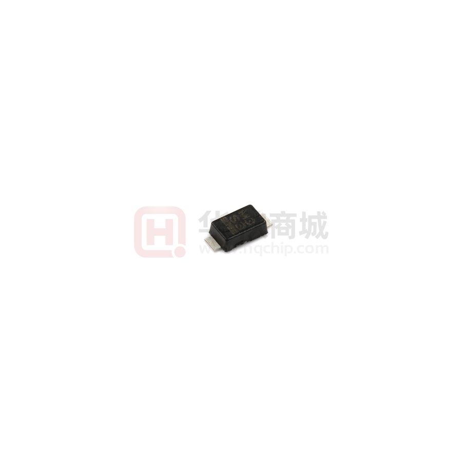
Case: SMF (DO-219AB)
Polarity: color band denotes cathode end
Weight: approx. 15 mg
Packaging codes / options:
GS18/10K per 13" reel (8 mm tape), MOQ = 50K
GS08/3K per 7" reel (8 mm tape), MOQ = 30K
• Material categorization: for definitions of compliance
please see www.vishay.com/doc?99912
Circuit configuration: single
PARTS TABLE
PART
ORDERING CODE
MARKING
REMARKS
SL02
SL02-GS18 or SL02-GS08
S2
Tape and reel
SL03
SL03-GS18 or SL03-GS08
S3
Tape and reel
ABSOLUTE MAXIMUM RATINGS (Tamb = 25 °C, unless otherwise specified)
PARAMETER
TEST CONDITION
Maximum repetitive peak reverse voltage
Maximum RMS voltage
Maximum DC blocking voltage
Maximum average forward rectified current
PART
SYMBOL
VALUE
UNIT
SL02
VRRM
20
V
SL03
VRRM
30
V
SL02
VRMS
14
V
SL03
VRMS
21
V
SL02
VDC
20
V
SL03
VDC
30
V
IF(AV)
1.1
A
IFSM
40
A
TL = 109 °C
Peak forward surge current 8.3 ms single
half sine-wave
THERMAL CHARACTERISTICS (Tamb = 25 °C, unless otherwise specified)
PARAMETER
TEST CONDITION
Thermal resistance junction to ambient air (1)
Maximum operating junction temperature
Storage temperature range
SYMBOL
VALUE
UNIT
RthJA
180
K/W
Tj
125
°C
Tstg
-55 to +150
°C
Note
(1) Mounted on epoxy substrate with 3 mm x 3 mm Cu pads ( 40 μm thick)
Rev. 2.3, 24-Oct-2019
Document Number: 85687
1
For technical questions within your region: DiodesAmericas@vishay.com, DiodesAsia@vishay.com, DiodesEurope@vishay.com
THIS DOCUMENT IS SUBJECT TO CHANGE WITHOUT NOTICE. THE PRODUCTS DESCRIBED HEREIN AND THIS DOCUMENT
ARE SUBJECT TO SPECIFIC DISCLAIMERS, SET FORTH AT www.vishay.com/doc?91000
�SL02, SL03
www.vishay.com
Vishay Semiconductors
ELECTRICAL CHARACTERISTICS (Tamb = 25 °C, unless otherwise specified)
PARAMETER
TEST CONDITION
IF = 0.5 A (1)
Instantaneous forward voltage
IF = 1.1 A
Typical instantaneous forward voltage
TA = 25 °C
Maximum DC reverse current at rated
DC blocking voltage
PART
SYMBOL
MIN.
TYP.
MAX.
UNIT
V
SL02
VF
0.360
0.385
SL03
VF
0.395
0.43
SL02
VF
0.420
SL03
VF
0.450
SL02
IR
V
V
V
250
μA
mA
TA = 100 °C
SL02
IR
8
TA = 25 °C
SL03
IR
130
μA
TA = 100 °C
SL03
IR
6
mA
SL02
trr
< 10
ns
SL03
trr
< 10
ns
Reverse recovery time
Note
(1) Pulse test: 300 μs pulse width, 1 % duty cycle
TYPICAL CHARACTERISTICS (Tamb = 25 °C, unless otherwise specified)
10
Instantaneous Forward Current (A)
Average Forward Current (A)
1.5
1.0
0.5
0
0 10
30
17379
50
70
90
Tj = 50 °C
0.01
Tj = 25 °C
0.001
Pulse width = 300 µs
1 % duty cycle
0
17381
Fig. 1 - Forward Current Derating Curve
0.8
0.2
1.0
0.4
0.6
Instantaneous Forward Voltage (V)
Fig. 3 - Typical Instantaneous Forward Characteristics - SL02
250
10 000
Instantaneous Reverse Current (µA)
Junction Capacitance (pF)
Tj = 75 °C
0.1
0.0001
110 130 150
Lead Temperature (°C)
200
150
100
SL02
50
Tj = 100 °C
Tj = 50 °C
100
Tj = 25 °C
10
1
0
2
6
8
4
Reverse Voltage (V)
10
12
Fig. 2 - Typical Junction Capacitance
Tj = 75 °C
1000
10
17380_SL02
Tj = 100 °C
1
17382
0
5
15
20
10
Reverse Voltage (V)
25
Fig. 4 - Typical Reverse Current Characteristics - SL02
Rev. 2.3, 24-Oct-2019
Document Number: 85687
2
For technical questions within your region: DiodesAmericas@vishay.com, DiodesAsia@vishay.com, DiodesEurope@vishay.com
THIS DOCUMENT IS SUBJECT TO CHANGE WITHOUT NOTICE. THE PRODUCTS DESCRIBED HEREIN AND THIS DOCUMENT
ARE SUBJECT TO SPECIFIC DISCLAIMERS, SET FORTH AT www.vishay.com/doc?91000
�SL02, SL03
www.vishay.com
Vishay Semiconductors
10 000
Instantaneous Reverse Current (µA)
Instantaneous Forward Current (A)
10
Tj = 100 °C
1
Tj = 75 °C
0.1
Tj = 50 °C
0.01
Tj = 25 °C
0.001
Pulse width = 300 µs
1 % duty cycle
0.0001
0
17383
Tj = 100 °C
1000
Tj = 75 °C
100
Tj = 50 °C
10
Tj = 25 °C
1
0.1
0.8
0.6
1.0
0.4
0.2
Instantaneous Forward Voltage (V)
0
10 15
20 25
Reverse Voltage (V)
5
17384
Fig. 5 - Typical Instantaneous Forward Characteristics - SL03
30
35
Fig. 6 - Typical Reverse Current Characteristics - SL03
PACKAGE DIMENSIONS in millimeters (inches): SMF (DO-219AB)
0.85 (0.033)
0 (0.000)
0.1 (0.004)
5
5
0.1(0.003)
1.7 (0.067)
Detail Z
enlarged
1.2 (0.047)
0.8 (0.031)
0.25 (0.010)
1.9 (0.075)
0.35 (0.014)
1.08 (0.043)
2.9 (0.114)
0.88 (0.035)
2.7 (0.106)
3.9 (0.154)
3.5 (0.138)
Foot print recommendation:
Created - Date: 15. February 2005
Rev. 3 - Date: 13. March 2007
Document no.: S8-V-3915.01-001 (4)
1.3 (0.051)
1.4 (0.055)
1.3 (0.051)
2.9 (0.114)
17247
Rev. 2.3, 24-Oct-2019
Document Number: 85687
3
For technical questions within your region: DiodesAmericas@vishay.com, DiodesAsia@vishay.com, DiodesEurope@vishay.com
THIS DOCUMENT IS SUBJECT TO CHANGE WITHOUT NOTICE. THE PRODUCTS DESCRIBED HEREIN AND THIS DOCUMENT
ARE SUBJECT TO SPECIFIC DISCLAIMERS, SET FORTH AT www.vishay.com/doc?91000
�SL02, SL03
www.vishay.com
Vishay Semiconductors
BLISTERTAPE DIMENSION in millimeters: SMF (DO-219AB)
PS
Document-No.: S8-V-3717.02-001 (3)
18513
Rev. 2.3, 24-Oct-2019
Document Number: 85687
4
For technical questions within your region: DiodesAmericas@vishay.com, DiodesAsia@vishay.com, DiodesEurope@vishay.com
THIS DOCUMENT IS SUBJECT TO CHANGE WITHOUT NOTICE. THE PRODUCTS DESCRIBED HEREIN AND THIS DOCUMENT
ARE SUBJECT TO SPECIFIC DISCLAIMERS, SET FORTH AT www.vishay.com/doc?91000
�SL02, SL03
www.vishay.com
Vishay Semiconductors
ORIENTATION IN CARRIER TAPE - SMF (DO-219AB)
Unreeling direction
SMF
cathode
Top view
Document no.: S8-V-3717.02-003 (4)
Created - Date: 09. Feb. 2010
22670
Rev. 2.3, 24-Oct-2019
Document Number: 85687
5
For technical questions within your region: DiodesAmericas@vishay.com, DiodesAsia@vishay.com, DiodesEurope@vishay.com
THIS DOCUMENT IS SUBJECT TO CHANGE WITHOUT NOTICE. THE PRODUCTS DESCRIBED HEREIN AND THIS DOCUMENT
ARE SUBJECT TO SPECIFIC DISCLAIMERS, SET FORTH AT www.vishay.com/doc?91000
�Legal Disclaimer Notice
www.vishay.com
Vishay
Disclaimer
ALL PRODUCT, PRODUCT SPECIFICATIONS AND DATA ARE SUBJECT TO CHANGE WITHOUT NOTICE TO IMPROVE
RELIABILITY, FUNCTION OR DESIGN OR OTHERWISE.
Vishay Intertechnology, Inc., its affiliates, agents, and employees, and all persons acting on its or their behalf (collectively,
“Vishay”), disclaim any and all liability for any errors, inaccuracies or incompleteness contained in any datasheet or in any other
disclosure relating to any product.
Vishay makes no warranty, representation or guarantee regarding the suitability of the products for any particular purpose or
the continuing production of any product. To the maximum extent permitted by applicable law, Vishay disclaims (i) any and all
liability arising out of the application or use of any product, (ii) any and all liability, including without limitation special,
consequential or incidental damages, and (iii) any and all implied warranties, including warranties of fitness for particular
purpose, non-infringement and merchantability.
Statements regarding the suitability of products for certain types of applications are based on Vishay’s knowledge of
typical requirements that are often placed on Vishay products in generic applications. Such statements are not binding
statements about the suitability of products for a particular application. It is the customer’s responsibility to validate that a
particular product with the properties described in the product specification is suitable for use in a particular application.
Parameters provided in datasheets and / or specifications may vary in different applications and performance may vary over
time. All operating parameters, including typical parameters, must be validated for each customer application by the customer’s
technical experts. Product specifications do not expand or otherwise modify Vishay’s terms and conditions of purchase,
including but not limited to the warranty expressed therein.
Except as expressly indicated in writing, Vishay products are not designed for use in medical, life-saving, or life-sustaining
applications or for any other application in which the failure of the Vishay product could result in personal injury or death.
Customers using or selling Vishay products not expressly indicated for use in such applications do so at their own risk.
Please contact authorized Vishay personnel to obtain written terms and conditions regarding products designed for
such applications.
No license, express or implied, by estoppel or otherwise, to any intellectual property rights is granted by this document
or by any conduct of Vishay. Product names and markings noted herein may be trademarks of their respective owners.
© 2019 VISHAY INTERTECHNOLOGY, INC. ALL RIGHTS RESERVED
Revision: 01-Jan-2019
1
Document Number: 91000
�