SMBJ5.0D thru SMBJ188D, SMBJ5.0CD thru SMBJ120CD
www.vishay.com
Vishay General Semiconductor
Surface-Mount TRANSZORB® Transient Voltage Suppressors
FEATURES
• Low profile package
• Ideal for automated placement
• ± 3.5 %: very tight VBR tolerance
• Low leakage current
• Available in unidirectional and bidirectional
• 600 W peak pulse power capability with a 10/1000 μs
waveform, repetitive rate (duty cycle): 0.01 %
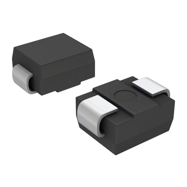
SMB (DO-214AA)
• Excellent clamping capability
• Very fast response time
LINKS TO ADDITIONAL RESOURCES
• Low incremental surge resistance
• Meets MSL level 1, per J-STD-020, LF maximum peak
of 260 °C
3D 3D
3D Models
• Material categorization: for definitions of compliance
please see www.vishay.com/doc?99912
PRIMARY CHARACTERISTICS
TYPICAL APPLICATIONS
VBR (unidirectional)
6.5 V to 228 V
VBR (bidirectional)
6.5 V to 145 V
VWM (unidirectional)
5.0 V to 188 V
VWM (bidirectional)
5.0 V to 120 V
PPPM
600 W
MECHANICAL DATA
PD at TM = 50 °C
5.0 W
PD at TA = 25 °C
1.0 W
TJ max.
150 °C
Polarity
Unidirectional, bidirectional
Case: SMB (DO-214AA)
Molding compound meets UL 94 V-0 flammability rating
Base P/N-M3 - halogen-free, RoHS-compliant, and
industrial grade
Package
SMB (DO-214AA)
DEVICES FOR BIDIRECTIONAL APPLICATIONS
For bidirectional devices use CD suffix (e.g. SMBJ5.0CD).
Electrical characteristics apply in both directions.
Use in sensitive electronics protection against voltage
transients induced by inductive load switching and lighting
on ICs, MOSFETs, signal lines of sensor units for consumer,
computer, industrial, and telecommunication.
Terminals: matte tin plated leads, solderable
J-STD-002 and JESD 22-B102
M3 suffix meets JESD 201 class 2 whisker test
per
Polarity: for unidirectional types the band denotes cathode
end, no cathode band on bidirectional types
MAXIMUM RATINGS (TA = 25 °C unless otherwise noted)
PARAMETER
Peak pulse power dissipation
Peak pulse current
Power dissipation
SYMBOL
VALUE
UNIT
with a 10/1000 μs waveform
PPPM (1)
600
W
with a 10/1000 μs waveform
(1)
See next table
A
IPPM
TM = 50 °C
PD (2)
5.0
TA = 25 °C
PD (3)
1.0
TJ, TSTG
-55 to +150
Operating junction and storage temperature range
W
°C
Notes
(1) Non-repetitive current pulse, per fig. 3 and derated above T = 25 °C per fig. 2
A
(2) Power dissipation mounted on infinite heatsink
(3) Power dissipation mounted on minimum recommended pad layout
Revision: 20-Jul-2020
Document Number: 87606
1
For technical questions within your region: DiodesAmericas@vishay.com, DiodesAsia@vishay.com, DiodesEurope@vishay.com
THIS DOCUMENT IS SUBJECT TO CHANGE WITHOUT NOTICE. THE PRODUCTS DESCRIBED HEREIN AND THIS DOCUMENT
ARE SUBJECT TO SPECIFIC DISCLAIMERS, SET FORTH AT www.vishay.com/doc?91000
�SMBJ5.0D thru SMBJ188D, SMBJ5.0CD thru SMBJ120CD
www.vishay.com
Vishay General Semiconductor
ELECTRICAL CHARACTERISTICS (TA = 25 °C unless otherwise noted)
DEVICE TYPE
(+)SMBJ5.0D
(+)SMBJ6.0D
(+)SMBJ6.5D
(+)SMBJ7.0D
(+)SMBJ7.5D
(+)SMBJ8.0D
(+)SMBJ8.5D
(+)SMBJ9.0D
(+)SMBJ10D
(+)SMBJ11D
(+)SMBJ12D
(+)SMBJ13D
(+)SMBJ14D
(+)SMBJ15D
(+)SMBJ16D
(+)SMBJ17D
(+)SMBJ18D
(+)SMBJ20D
(+)SMBJ22D
(+)SMBJ24D
(+)SMBJ26D
(+)SMBJ28D
(+)SMBJ30D
(+)SMBJ33D
(+)SMBJ36D
(+)SMBJ40D
(+)SMBJ43D
(+)SMBJ45D
(+)SMBJ48D
(+)SMBJ51D
(+)SMBJ54D
(+)SMBJ58D
(+)SMBJ60D
(+)SMBJ64D
(+)SMBJ70D
(+)SMBJ75D
(+)SMBJ78D
(+)SMBJ85D
(+)SMBJ90D
(+)SMBJ100D
(+)SMBJ110D
(+)SMBJ120D
(+)SMBJ130D
(+)SMBJ150D
(+)SMBJ160D
(+)SMBJ170D
SMBJ188D
DEVICE
MARKING
CODE
UNI
6AA
6AB
6AC
6AD
6AE
6AF
6AG
6AH
6AK
6AL
6AM
6AN
6AP
6AQ
6AR
6AS
6AT
6AU
6AV
6AW
6AX
6AY
6AZ
6BA
6BB
6BC
6BD
6BE
6BF
6BG
6BH
6BK
6BL
6BM
6BN
6BP
6BQ
6BR
6BS
6BT
6BU
6BV
6BW
6BX
6BY
6BZ
6CA
BI
6AA
6AB
6AC
6AD
6AE
6AF
6AG
6AH
6AK
6AL
6AM
6AN
6AP
6AQ
6AR
6AS
6AT
6AU
6AV
6AW
6AX
6AY
6AZ
6BA
6BB
6BC
6BD
6BE
6BF
6BG
6BH
6BK
6BL
6BM
6BN
6BP
6BQ
6BR
6BS
6BT
6BU
6BV
-
BREAKDOWN
VOLTAGE
VBR AT IT (1)
(V)
MIN.
MAX.
6.50
6.97
6.77
7.27
7.33
7.87
7.90
8.48
8.46
9.08
9.03
9.69
9.57
10.3
10.2
10.9
11.3
12.1
12.4
13.3
13.5
14.5
14.6
15.7
15.8
17.0
17.0
18.2
18.1
19.4
19.2
20.6
20.3
21.8
22.5
24.2
24.8
26.6
27.1
29.1
29.3
31.5
31.6
33.9
33.8
36.3
37.3
40.0
40.6
43.6
45.1
48.4
48.5
52.1
50.8
54.5
54.1
58.1
57.6
61.8
60.9
65.4
65.4
70.2
67.7
72.7
72.2
77.5
79.0
84.8
84.6
90.8
88.1
94.4
95.7
103
102
109
113
121
124
133
135
145
146
157
170
182
181
194
192
206
212
228
TEST
CURRENT
IT
(mA)
STAND-OFF
VOLTAGE
VWM (V)
MAXIMUM
REVERSE
LEAKAGE
AT VWM
ID (μA) (2)
MAXIMUM
PEAK PULSE
SURGE
CURRENT
IPPM (A) (3)
MAXIMUM
CLAMPING
VOLTAGE
AT IPPM
VC (V)
10
10
10
10
1.0
1.0
1.0
1.0
1.0
1.0
1.0
1.0
1.0
1.0
1.0
1.0
1.0
1.0
1.0
1.0
1.0
1.0
1.0
1.0
1.0
1.0
1.0
1.0
1.0
1.0
1.0
1.0
1.0
1.0
1.0
1.0
1.0
1.0
1.0
1.0
1.0
1.0
1.0
1.0
1.0
1.0
1.0
5.0
6.0
6.5
7.0
7.5
8.0
8.5
9.0
10
11
12
13
14
15
16
17
18
20
22
24
26
28
30
33
36
40
43
45
48
51
54
58
60
64
70
75
78
85
90
100
110
120
130
150
160
170
188
500
500
300
150
75
35
15
5.0
2.0
2.0
2.0
0.5
0.5
0.5
0.5
0.5
0.5
0.5
0.5
0.5
0.5
0.5
0.5
0.5
0.5
0.5
0.5
0.5
0.5
0.5
0.5
0.5
0.5
0.5
0.5
0.5
0.5
0.5
0.5
0.5
0.5
0.5
0.5
0.5
0.5
0.5
0.5
65.9
58.9
54.5
50.8
47.2
44.8
42.2
39.7
35.9
33.5
30.6
28.3
26.2
25.0
23.4
22.1
20.8
18.8
17.1
15.6
14.5
13.4
12.6
11.5
10.5
9.43
8.76
8.40
7.90
7.40
7.00
6.50
6.28
5.88
5.40
5.06
4.86
4.46
4.17
3.77
3.45
3.15
2.94
2.53
2.34
2.23
2.03
9.1
10.2
11.0
11.8
12.7
13.4
14.3
15.1
16.7
17.9
19.6
21.2
22.9
24.0
25.6
27.2
28.8
32.0
35.1
38.4
41.6
44.7
47.7
52.5
57.3
63.6
68.5
71.6
76.3
81.2
85.9
92.3
95.5
102
111
119
124
135
144
159
174
190
206
239
256
270
301
Notes
• All terms and symbols are consistent with ANSI/IEEE C62.35
(1) Pulse test: t ≤ 50 ms
p
(2) For bi-directional types having V
WM of 12 V and less, the ID limit is doubled
(3) Surge current waveform per fig. 3 and derate per fig. 2
(+) Underwriters Laboratory Recognition for the classification of protectors (QVGQ2) under the UL standard for safety 497B and file number
E136766 for both uni-directional and bi-directional device
Revision: 20-Jul-2020
Document Number: 87606
2
For technical questions within your region: DiodesAmericas@vishay.com, DiodesAsia@vishay.com, DiodesEurope@vishay.com
THIS DOCUMENT IS SUBJECT TO CHANGE WITHOUT NOTICE. THE PRODUCTS DESCRIBED HEREIN AND THIS DOCUMENT
ARE SUBJECT TO SPECIFIC DISCLAIMERS, SET FORTH AT www.vishay.com/doc?91000
�SMBJ5.0D thru SMBJ188D, SMBJ5.0CD thru SMBJ120CD
www.vishay.com
Vishay General Semiconductor
THERMAL CHARACTERISTICS (TA = 25 °C unless otherwise noted)
PARAMETER
Typical thermal resistance, junction to ambient
Typical thermal resistance, junction to mount
SYMBOL
VALUE
RθJA (1)
125
RθJA (2)
100
RθJM
20
UNIT
°C/W
Notes
(1) Mounted on minimum recommended pad layout
(2) Mounted on 5.0 mm x 5.0 mm copper pad area
ORDERING INFORMATION (Example)
PREFERRED P/N
UNIT WEIGHT (g)
PREFERRED PACKAGE CODE
BASE QUANTITY
DELIVERY MODE
SMBJ5.0D-M3/H
0.096
H
750
7" diameter plastic tape and reel
SMBJ5.0D-M3/I
0.096
I
3200
13" diameter plastic tape and reel
RATINGS AND CHARACTERISTICS CURVES (TA = 25 °C unless otherwise noted)
150
IPPM - Peak Pulse Current, % IRSM
PPPM - Peak Pulse Power (kW)
10
1
0.2" x 0.2" (5.0 mm x 5.0 mm)
copper pad areas
0.1
tr = 10 μs
100
Peak value IPPM
Half value - IPP/2
50
10/1000 μs waveform
as de ned by R.E.A.
td
0
10
100
1000
0
10 000
td - Pulse Width (μs)
0.5
1.0
1.5
2.0
2.5
3.0
3.5
4.0
tp - Time (ms)
Fig. 1 - Peak Pulse Power Rating Curve
Fig. 3 - Pulse Waveform
100
10000
CJ - Junction Capacitance (pF)
Peak Pulse Power (PPP) or Current (IPP)
Derating in Percentage, %
TJ = 25 °C
pulse width (td) is de ned
as the point where the peak
current decays to 50 % of IPPM
75
50
25
0
Measured at zero bias
1000
100
Measured at stand-off
voltage, VWM
10
Uni-Directional
Bi-Directional
TJ = 25 °C
f = 1.0 MHz
1
0
25
50
75
100
125
150
TJ - Initial Temperature (°C)
Fig. 2 - Pulse Power or Current vs. Initial Junction Temperature
1
10
100
VWM - Reverse Stand-Off Voltage (V)
Fig. 4 - Typical Junction Capacitance
Revision: 20-Jul-2020
Document Number: 87606
3
For technical questions within your region: DiodesAmericas@vishay.com, DiodesAsia@vishay.com, DiodesEurope@vishay.com
THIS DOCUMENT IS SUBJECT TO CHANGE WITHOUT NOTICE. THE PRODUCTS DESCRIBED HEREIN AND THIS DOCUMENT
ARE SUBJECT TO SPECIFIC DISCLAIMERS, SET FORTH AT www.vishay.com/doc?91000
�SMBJ5.0D thru SMBJ188D, SMBJ5.0CD thru SMBJ120CD
Vishay General Semiconductor
6
Transient Thermal Impedance (°C/W)
PM(av) - Steady State Power Dissipation (W)
www.vishay.com
TA=TM mounted on inifinite heatsink
5
4
3
2
Mounted on minimum
recommend pad layout
1
0
0
25
50
75
100
125
150
1000
Junction to Ambient
100
Mounted on minimum
recommend pad area
10
1
Mounted on 5.0 x 5.0 mm
copper pad area
0.1
0.001
0.1
10
1000
tp - Pulse Duration (s)
TA - Ambient Temperature (°C)
Fig. 5 - Power Dissipation Derating Curve
Fig. 6 - Typical Transient Thermal Impedance
Note
• Fig.1, 10 000 μs Pppm is actual test for VWM ≤ 60 V types, over 60 V types 10 000 μs Pppm is curve extensional value
PACKAGE OUTLINE DIMENSIONS in inches (millimeters)
SMB (DO-214AA)
Cathode Band
Mounting Pad Layout
0.085 (2.159) MAX.
0.155 (3.94)
0.130 (3.30)
0.086 (2.20)
0.077 (1.95)
0.086 (2.18) MIN.
0.180 (4.57)
0.160 (4.06)
0.060 (1.52) MIN.
0.012 (0.305)
0.006 (0.152)
0.220 (5.59) REF.
0.096 (2.44)
0.084 (2.13)
0.060 (1.52)
0.030 (0.76)
0.008 (0.2)
0 (0)
0.220 (5.59)
0.205 (5.21)
Revision: 20-Jul-2020
Document Number: 87606
4
For technical questions within your region: DiodesAmericas@vishay.com, DiodesAsia@vishay.com, DiodesEurope@vishay.com
THIS DOCUMENT IS SUBJECT TO CHANGE WITHOUT NOTICE. THE PRODUCTS DESCRIBED HEREIN AND THIS DOCUMENT
ARE SUBJECT TO SPECIFIC DISCLAIMERS, SET FORTH AT www.vishay.com/doc?91000
�Legal Disclaimer Notice
www.vishay.com
Vishay
Disclaimer
ALL PRODUCT, PRODUCT SPECIFICATIONS AND DATA ARE SUBJECT TO CHANGE WITHOUT NOTICE TO IMPROVE
RELIABILITY, FUNCTION OR DESIGN OR OTHERWISE.
Vishay Intertechnology, Inc., its affiliates, agents, and employees, and all persons acting on its or their behalf (collectively,
“Vishay”), disclaim any and all liability for any errors, inaccuracies or incompleteness contained in any datasheet or in any other
disclosure relating to any product.
Vishay makes no warranty, representation or guarantee regarding the suitability of the products for any particular purpose or
the continuing production of any product. To the maximum extent permitted by applicable law, Vishay disclaims (i) any and all
liability arising out of the application or use of any product, (ii) any and all liability, including without limitation special,
consequential or incidental damages, and (iii) any and all implied warranties, including warranties of fitness for particular
purpose, non-infringement and merchantability.
Statements regarding the suitability of products for certain types of applications are based on Vishay's knowledge of typical
requirements that are often placed on Vishay products in generic applications. Such statements are not binding statements
about the suitability of products for a particular application. It is the customer's responsibility to validate that a particular product
with the properties described in the product specification is suitable for use in a particular application. Parameters provided in
datasheets and / or specifications may vary in different applications and performance may vary over time. All operating
parameters, including typical parameters, must be validated for each customer application by the customer's technical experts.
Product specifications do not expand or otherwise modify Vishay's terms and conditions of purchase, including but not limited
to the warranty expressed therein.
Hyperlinks included in this datasheet may direct users to third-party websites. These links are provided as a convenience and
for informational purposes only. Inclusion of these hyperlinks does not constitute an endorsement or an approval by Vishay of
any of the products, services or opinions of the corporation, organization or individual associated with the third-party website.
Vishay disclaims any and all liability and bears no responsibility for the accuracy, legality or content of the third-party website
or for that of subsequent links.
Except as expressly indicated in writing, Vishay products are not designed for use in medical, life-saving, or life-sustaining
applications or for any other application in which the failure of the Vishay product could result in personal injury or death.
Customers using or selling Vishay products not expressly indicated for use in such applications do so at their own risk. Please
contact authorized Vishay personnel to obtain written terms and conditions regarding products designed for such applications.
No license, express or implied, by estoppel or otherwise, to any intellectual property rights is granted by this document or by
any conduct of Vishay. Product names and markings noted herein may be trademarks of their respective owners.
© 2023 VISHAY INTERTECHNOLOGY, INC. ALL RIGHTS RESERVED
Revision: 01-Jan-2023
1
Document Number: 91000
�