SUD45P04-16P
Vishay Siliconix
P-Channel 40 V (D-S) MOSFET
FEATURES
PRODUCT SUMMARY
VDS (V)
- 40
RDS(on) () Max.
ID (A)
0.0162 at VGS = - 10 V
- 36
0.0230 at VGS = - 4.5 V
- 24
Qg (Typ.)
67
• Halogen-free According to IEC 61249-2-21
Definition
• TrenchFET® Power MOSFET
• 100 % Rg and UIS Tested
• Compliant to RoHS Directive 2002/95/EC
APPLICATIONS
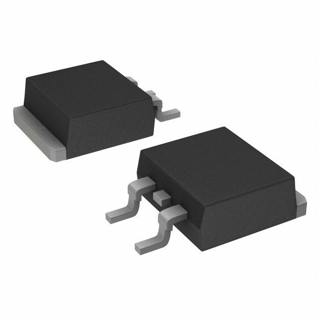
TO-252
• Power Switch
• Load Switch in High Current Applications
• DC/DC Converters
S
Drain Connected to Tab
G
D
S
G
Top View
Ordering Information:
SUD45P04-16P-GE3 (Lead (Pb)-free and Halogen-free)
P-Channel MOSFET
D
ABSOLUTE MAXIMUM RATINGS (TC = 25 °C, unless otherwise noted)
Parameter
Symbol
Limit
Drain-Source Voltage
VDS
- 40
Gate-Source Voltage
VGS
± 20
Continuous Drain Current (TJ = 150 °C)
TC = 25 °C
TC = 70 °C
Pulsed Drain Current (t = 300 µs)
Avalanche Current
Single Avalanche Energya
Maximum Power Dissipationa
Operating Junction and Storage Temperature Range
L = 0.1 mH
TC = 25 °C
TA = 25 °Cc
ID
V
- 36
- 29
IDM
- 100
IAS
- 32
EAS
51
PD
Unit
41.7
A
mJ
b
2.1
W
TJ, Tstg
- 55 to 150
°C
Unit
THERMAL RESISTANCE RATINGS
Parameter
Symbol
Limit
Junction-to-Ambient (PCB Mount)c
RthJA
60
Junction-to-Case (Drain)
RthJC
3
°C/W
Notes:
a. Duty cycle 1 %.
b. See SOA curve for voltage derating.
c. When mounted on 1" square PCB (FR-4 material).
Document Number: 63372
S11-1657-Rev. A, 15-Aug-11
www.vishay.com
1
This document is subject to change without notice.
THE PRODUCTS DESCRIBED HEREIN AND THIS DOCUMENT ARE SUBJECT TO SPECIFIC DISCLAIMERS, SET FORTH AT www.vishay.com/doc?91000
�SUD45P04-16P
Vishay Siliconix
SPECIFICATIONS (TJ = 25 °C, unless otherwise noted)
Parameter
Symbol
Test Conditions
Min.
VDS
VDS = 0 V, ID = - 250 µA
- 40
VGS(th)
VDS = VGS, ID = - 250 µA
-1
IGSS
VDS = 0 V, VGS = ± 20 V
Typ.
Max.
Unit
Static
Drain-Source Breakdown Voltage
Gate Threshold Voltage
Gate-Body Leakage
Zero Gate Voltage Drain Current
On-State Drain Currenta
Drain-Source On-State Resistancea
Forward Transconductancea
IDSS
- 2.5
± 250
VDS = - 40 V, VGS = 0 V
-1
VDS = - 40 V, VGS = 0 V, TJ = 125 °C
- 50
VDS = - 40 V, VGS = 0 V, TJ = 150 °C
- 250
VDS - 10 V, VGS = - 10 V
ID(on)
RDS(on)
gfs
- 50
V
nA
µA
A
VGS = - 10 V, ID = - 14 A
0.0135
0.0162
VGS = - 4.5 V, ID = - 12 A
0.0190
0.0230
VDS = - 20 V, ID = - 14 A
40
S
Dynamicb
Input Capacitance
Ciss
Output Capacitance
Coss
Reverse Transfer Capacitance
Crss
Total Gate Chargec
Qg
Gate-Source Chargec
Qgs
c
Gate-Drain Charge
67
VDS = - 20 V, VGS = - 10 V, ID = - 14 A
Rise Timec
Fall Timec
f = 1 MHz
td(on)
tr
c
td(off)
100
nC
13.5
14
Rg
Turn-On Delay Timec
pF
330
280
Qgd
Gate Resistance
Turn-Off Delay Time
2765
VGS = 0 V, VDS = - 20 V, f = 1 MHz
VDD = - 20 V, RL = 2
ID - 10 A, VGEN = - 10 V, Rg = 1
tf
Drain-Source Body Diode Ratings and Characteristics TC = 25 °C
0.5
2.5
5
10
20
11
20
42
63
12
20
- 36
Pulsed Current
ISM
- 100
Forward Voltagea
VSD
Reverse Recovery Time
Peak Reverse Recovery Current
Reverse Recovery Charge
IF = - 10 A, VGS = 0 V
- 0.8
IF = - 10 A, dI/dt = 100 A/µs
40
trr
IRM(REC)
Qrr
ns
b
IS
Continuous Current
A
- 1.5
V
38
57
ns
2.3
3.5
A
60
nC
Notes:
a. Pulse test; pulse width 300 µs, duty cycle 2 %.
b. Guaranteed by design, not subject to production testing.
c. Independent of operating temperature.
Stresses beyond those listed under “Absolute Maximum Ratings” may cause permanent damage to the device. These are stress ratings only, and functional operation
of the device at these or any other conditions beyond those indicated in the operational sections of the specifications is not implied. Exposure to absolute maximum
rating conditions for extended periods may affect device reliability.
www.vishay.com
2
Document Number: 63372
S11-1657-Rev. A, 15-Aug-11
This document is subject to change without notice.
THE PRODUCTS DESCRIBED HEREIN AND THIS DOCUMENT ARE SUBJECT TO SPECIFIC DISCLAIMERS, SET FORTH AT www.vishay.com/doc?91000
�SUD45P04-16P
Vishay Siliconix
TYPICAL CHARACTERISTICS (25 °C, unless otherwise noted)
40
0.030
VGS = 10 V thru 4 V
0.025
RDS(on) - On-Resistance (Ω)
ID - Drain Current (A)
30
20
10
VGS = 3 V
VGS = 4.5 V
0.020
0.015
VGS = 10 V
0.010
0.005
0
0
0.5
1
1.5
0
2
20
40
60
ID - Drain Current (A)
VDS - Drain-to-Source Voltage (V)
Output Characteristics
80
100
On-Resistance vs. Drain Current
1.0
0.040
ID = 14 A
0.034
RDS(on) - On-Resistance (Ω)
ID - Drain Current (A)
0.8
0.6
TC = 25 °C
0.4
0.2
TC = 125 °C
TC = - 55 °C
0
0
0.7
1.4
2.1
2.8
0.028
0.016
TJ = 25 °C
0.010
2
3.5
4
6
8
10
VGS - Gate-to-Source Voltage (V)
VGS - Gate-to-Source Voltage (V)
Transfer Characteristics
On-Resistance vs. Gate-to-Source Voltage
50
10
TC = 25 °C
ID = 14 A
VGS - Gate-to-Source Voltage (V)
TC = - 55 °C
40
g fs - Transconductance (S)
TJ = 125 °C
0.022
30
TC = 125 °C
20
10
8
VDS = 20 V
6
VDS = 10 V
4
VDS = 32 V
2
0
0
0
6
12
18
ID - Drain Current (A)
Transconductance
Document Number: 63372
S11-1657-Rev. A, 15-Aug-11
24
30
0
14
28
42
56
70
Qg - Total Gate Charge (nC)
Gate Charge
www.vishay.com
3
This document is subject to change without notice.
THE PRODUCTS DESCRIBED HEREIN AND THIS DOCUMENT ARE SUBJECT TO SPECIFIC DISCLAIMERS, SET FORTH AT www.vishay.com/doc?91000
�SUD45P04-16P
Vishay Siliconix
TYPICAL CHARACTERISTICS (25 °C, unless otherwise noted)
2.3
100
2.0
TJ = 150 °C
10
VGS(th) (V)
IS - Source Current (A)
ID = 250 μA
1.7
TJ = 25 °C
1
1.4
1.1
- 50
0.1
0.0
0.2
0.4
0.6
0.8
1.0
1.2
- 25
0
25
50
75
100
VSD - Source-to-Drain Voltage (V)
TJ - Temperature (°C)
Source-Drain Diode Forward Voltage
Threshold Voltage
4300
125
150
125
150
51
VDS (V) Drain-to-Source Voltage
ID = 250 μA
C - Capacitance (pF)
3440
Ciss
2580
1720
860
Coss
49
47
45
Crss
43
- 50
0
0
10
20
30
VDS - Drain-to-Source Voltage (V)
40
- 25
0
25
50
75
100
TJ - Temperature (°C)
Capacitance
Drain Source Breakdown vs. Junction Temperature
2.2
40
VGS = 10 V
1.9
30
ID - Drain Current (A)
RDS(on) - On-Resistance (Normalized)
ID = 14 A
1.6
VGS = 4.5 V
1.3
20
10
1.0
0.7
- 50
0
- 25
0
25
50
75
100
125
150
TJ - Junction Temperature (°C)
50
75
100
TC - Case Temperature (°C)
On-Resistance vs. Junction Temperature
Current Derating
www.vishay.com
4
0
25
125
150
Document Number: 63372
S11-1657-Rev. A, 15-Aug-11
This document is subject to change without notice.
THE PRODUCTS DESCRIBED HEREIN AND THIS DOCUMENT ARE SUBJECT TO SPECIFIC DISCLAIMERS, SET FORTH AT www.vishay.com/doc?91000
�SUD45P04-16P
Vishay Siliconix
TYPICAL CHARACTERISTICS (25 °C, unless otherwise noted)
1000
100
IDAV (A)
TJ = 150 °C
ID - Drain Current (A)
100
TJ = 25 °C
10
100 μs
10
1 ms
Limited by R DS(on)*
10 ms
DC, 1 s, 100 ms
1
0.1
1
0.000001
TC = 25 °C
Single Pulse
0.01
0.00001
0.0001
0.001
0.01
0.1
0.1
Time (s)
Single Pulse Avalanche Current Capability vs. Time
BVDSS Limited
1
10
VDS - Drain-to-Source Voltage (V)
* VGS > minimum VGS at which RDS(on) is specified
100
Safe Operating Area
2
Normalized Effective Transient
Thermal Impedance
1
Duty Cycle = 0.5
0.2
0.1
0.1
0.02
0.05
Single Pulse
0.01
10-4
10-3
10-2
10-1
Square Wave Pulse Duration (s)
1
10
30
Normalized Thermal Transient Impedance, Junction-to-Case
Vishay Siliconix maintains worldwide manufacturing capability. Products may be manufactured at one of several qualified locations. Reliability data for Silicon
Technology and Package Reliability represent a composite of all qualified locations. For related documents such as package/tape drawings, part marking, and
reliability data, see www.vishay.com/ppg?63372.
Document Number: 63372
S11-1657-Rev. A, 15-Aug-11
www.vishay.com
5
This document is subject to change without notice.
THE PRODUCTS DESCRIBED HEREIN AND THIS DOCUMENT ARE SUBJECT TO SPECIFIC DISCLAIMERS, SET FORTH AT www.vishay.com/doc?91000
�Package Information
www.vishay.com
Vishay Siliconix
TO-252AA Case Outline
E
MILLIMETERS
A
C2
e
b2
D1
e1
E1
L
gage plane height (0.5 mm)
L4
b
L5
H
D
L3
b3
C
A1
INCHES
DIM.
MIN.
MAX.
MIN.
MAX.
A
2.18
2.38
0.086
0.094
A1
-
0.127
-
0.005
b
0.64
0.88
0.025
0.035
b2
0.76
1.14
0.030
0.045
b3
4.95
5.46
0.195
0.215
0.024
C
0.46
0.61
0.018
C2
0.46
0.89
0.018
0.035
D
5.97
6.22
0.235
0.245
D1
4.10
-
0.161
-
E
6.35
6.73
0.250
0.265
E1
4.32
-
0.170
-
H
9.40
10.41
0.370
0.410
e
2.28 BSC
e1
0.090 BSC
4.56 BSC
0.180 BSC
L
1.40
1.78
0.055
0.070
L3
0.89
1.27
0.035
0.050
L4
-
1.02
-
0.040
L5
1.01
1.52
0.040
0.060
ECN: T16-0236-Rev. P, 16-May-16
DWG: 5347
Notes
• Dimension L3 is for reference only.
Revision: 16-May-16
Document Number: 71197
1
For technical questions, contact: pmostechsupport@vishay.com
THIS DOCUMENT IS SUBJECT TO CHANGE WITHOUT NOTICE. THE PRODUCTS DESCRIBED HEREIN AND THIS DOCUMENT
ARE SUBJECT TO SPECIFIC DISCLAIMERS, SET FORTH AT www.vishay.com/doc?91000
�Application Note 826
Vishay Siliconix
RECOMMENDED MINIMUM PADS FOR DPAK (TO-252)
0.224
0.243
0.087
(2.202)
0.090
(2.286)
(10.668)
0.420
(6.180)
(5.690)
0.180
0.055
(4.572)
(1.397)
Recommended Minimum Pads
Dimensions in Inches/(mm)
Return to Index
Return to Index
APPLICATION NOTE
Document Number: 72594
Revision: 21-Jan-08
www.vishay.com
3
�Legal Disclaimer Notice
www.vishay.com
Vishay
Disclaimer
ALL PRODUCT, PRODUCT SPECIFICATIONS AND DATA ARE SUBJECT TO CHANGE WITHOUT NOTICE TO IMPROVE
RELIABILITY, FUNCTION OR DESIGN OR OTHERWISE.
Vishay Intertechnology, Inc., its affiliates, agents, and employees, and all persons acting on its or their behalf (collectively,
“Vishay”), disclaim any and all liability for any errors, inaccuracies or incompleteness contained in any datasheet or in any other
disclosure relating to any product.
Vishay makes no warranty, representation or guarantee regarding the suitability of the products for any particular purpose or
the continuing production of any product. To the maximum extent permitted by applicable law, Vishay disclaims (i) any and all
liability arising out of the application or use of any product, (ii) any and all liability, including without limitation special,
consequential or incidental damages, and (iii) any and all implied warranties, including warranties of fitness for particular
purpose, non-infringement and merchantability.
Statements regarding the suitability of products for certain types of applications are based on Vishay’s knowledge of typical
requirements that are often placed on Vishay products in generic applications. Such statements are not binding statements
about the suitability of products for a particular application. It is the customer’s responsibility to validate that a particular
product with the properties described in the product specification is suitable for use in a particular application. Parameters
provided in datasheets and/or specifications may vary in different applications and performance may vary over time. All
operating parameters, including typical parameters, must be validated for each customer application by the customer’s
technical experts. Product specifications do not expand or otherwise modify Vishay’s terms and conditions of purchase,
including but not limited to the warranty expressed therein.
Except as expressly indicated in writing, Vishay products are not designed for use in medical, life-saving, or life-sustaining
applications or for any other application in which the failure of the Vishay product could result in personal injury or death.
Customers using or selling Vishay products not expressly indicated for use in such applications do so at their own risk. Please
contact authorized Vishay personnel to obtain written terms and conditions regarding products designed for such applications.
No license, express or implied, by estoppel or otherwise, to any intellectual property rights is granted by this document or by
any conduct of Vishay. Product names and markings noted herein may be trademarks of their respective owners.
Material Category Policy
Vishay Intertechnology, Inc. hereby certifies that all its products that are identified as RoHS-Compliant fulfill the
definitions and restrictions defined under Directive 2011/65/EU of The European Parliament and of the Council
of June 8, 2011 on the restriction of the use of certain hazardous substances in electrical and electronic equipment
(EEE) - recast, unless otherwise specified as non-compliant.
Please note that some Vishay documentation may still make reference to RoHS Directive 2002/95/EC. We confirm that
all the products identified as being compliant to Directive 2002/95/EC conform to Directive 2011/65/EU.
Vishay Intertechnology, Inc. hereby certifies that all its products that are identified as Halogen-Free follow Halogen-Free
requirements as per JEDEC JS709A standards. Please note that some Vishay documentation may still make reference
to the IEC 61249-2-21 definition. We confirm that all the products identified as being compliant to IEC 61249-2-21
conform to JEDEC JS709A standards.
Revision: 02-Oct-12
1
Document Number: 91000
�