SUD50P04-15
New Product
Vishay Siliconix
P-Channel 40-V (D-S), 175�C MOSFET
���
� � �������
VDS (V)
–40
rDS(on) (�)
ID (A)
0.015 @ VGS = –10 V
–50
0.023 @ VGS = –4.5 V
–45
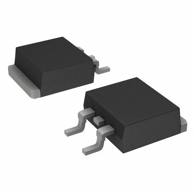
S
TO-252
G
Drain Connected to Tab
G
D
S
Top View
Order Number:
SUD50P04-15
D
P-Channel MOSFET
�������� ������� ������� ��� � ��� ������ ��
������ ����
�
Parameter
Symbol
Limit
Drain-Source Voltage
VDS
–40
Gate-Source Voltage
VGS
�20
TC = 25�C
Continuous Drain Currentb
TC = 100�C
Pulsed Drain Current
–40
A
Maximum Power Dissipationb
–150
IS
TC = 25�C
TA = 25�C
Operating Junction and Storage Temperature Range
V
–50
ID
IDM
Continuous Source Current (Diode Conduction)
Unit
–50
100b
PD
W
3a
TJ, Tstg
�C
–55 to 175
�
����� �������� � �������
Parameter
Maximum Junction-to-Ambienta
Symbol
t � 10 sec.
Steady State
Maximum Junction-to-Case
RthJA
RthJC
Typical
Maximum
15
18
40
50
1.2
1.5
Unit
�C/W
Notes
a. Surface Mounted on 1” x 1” FR4 Board.
b. See SOA curve for voltage derating.
Document Number: 71176
S-00830—Rev. A, 24-Apr-00
www.vishay.com � FaxBack 408-970-5600
1
�SUD50P04-15
New Product
Vishay Siliconix
��
�
�
���
��� ��� � ���� ���
�� ���
��
�
���
� �
Parameter
Symbol
Test Condition
Min
Typ
Max
V(BR)DSS
VGS = 0 V, ID = –250 mA
–40
VGS(th)
VDS = VGS, ID = –250 mA
–1.0
IGSS
VDS = 0 V, VGS = "20 V
"100
VDS = –40 V, VGS = 0 V
–1
VDS = –40 V, VGS = 0 V, TJ = 125�C
–50
Unit
Static
Drain-Source Breakdown Voltage
Gate Threshold Voltage
Gate-Body Leakage
Zero Gate Voltage Drain Current
On-State Drain Currenta
IDSS
ID(on)
VDS = –5 V, VGS = –10 V
V
–120
VGS = –10 V, ID = –30 A
a
Drain-Source
On-State
Resistance
D i S
O S
R i
rDS(on)
Forward Transconductancea
gfs
VGS = –10 V, ID = –30 A, TJ = 125�C
VDS = –15 V, ID = –30 A
mA
A
0.012
0.015
0.024
VGS = –4.5 V, ID = –20 A
nA
0.018
W
0.023
20
S
Dynamicb
Input Capacitance
Ciss
Output Capacitance
Coss
Reverse Transfer Capacitance
Crss
5400
VGS = 0 V, VDS = –25 V, f = 1 MHz
pF
F
640
300
Total Gate Chargec
Qg
Gate-Source Chargec
Qgs
Gate-Drain Chargec
Qgd
Turn-On Delay Timec
td(on)
15
25
tr
380
580
75
115
140
210
Rise Timec
Turn-Off Delay Timec
Fall Timec
td(off)
85
VDS = –20
V, VGS = –10
V, ID = –50
20 V
10 V
50 A
130
nC
C
25
15
VDD = –20
20 V
V,, RL = 0
0.4
4W
ID ^ –50
50 A,
A VGEN = –10
10 V
V, RG = 2
2.5
5W
tf
ns
Source-Drain Diode Ratings and Characteristic (TC = 25�C)
Pulsed Current
ISM
–150
A
Diode Forward Voltagea
VSD
IF = –50 A, VGS = 0 V
–1.2
–1.5
V
trr
IF = –50 A, di/dt = 100 A/ms
40
80
ns
Source-Drain Reverse Recovery Time
Notes
a. Pulse test; pulse width v 300 ms, duty cycle v 2%.
b. Guaranteed by design, not subject to production testing.
c. Independent of operating temperature.
www.vishay.com � FaxBack 408-970-5600
2
Document Number: 71176
S-00830—Rev. A, 24-Apr-00
�SUD50P04-15
New Product
Vishay Siliconix
������� �
����� ������� ����� �
� ��
�� ��
Output Characteristics
Transfer Characteristics
250
100
7V
VGS = 10, 9, 8 V
TC = –55�C
6V
200
80
I D – Drain Current (A)
I D – Drain Current (A)
25�C
150
5V
100
4V
50
125�C
60
40
20
2, 3 V
0
0
0
2
4
6
8
10
0
VDS – Drain-to-Source Voltage (V)
1
2
3
4
5
6
VGS – Gate-to-Source Voltage (V)
Transconductance
On-Resistance vs. Drain Current
80
0.04
TC = –55�C
r DS(on) – On-Resistance ( Ω )
g fs – Transconductance (S)
25�C
60
125�C
40
20
0
0.03
VGS = 4.5 V
0.02
VGS = 10 V
0.01
0
0
20
40
60
80
100
0
20
40
ID – Drain Current (A)
80
100
120
ID – Drain Current (A)
Capacitance
Gate Charge
8000
V GS – Gate-to-Source Voltage (V)
20
Ciss
6000
C – Capacitance (pF)
60
4000
2000
Coss
Crss
0
VDS = 20 V
ID = 50 A
16
12
8
4
0
0
5
10
15
20
25
VDS – Drain-to-Source Voltage (V)
Document Number: 71176
S-00830—Rev. A, 24-Apr-00
30
0
40
80
120
160
Qg – Total Gate Charge (nC)
www.vishay.com � FaxBack 408-970-5600
3
�SUD50P04-15
New Product
Vishay Siliconix
������
������� ������� ����� ��
�� ��� ��
On-Resistance vs. Junction Temperature
Source-Drain Diode Forward Voltage
2.5
100
2.0
I S – Source Current (A)
r DS(on) – On-Resistance ( Ω )
(Normalized)
VGS = 10 V
ID = 30 A
1.5
1.0
TJ = 150�C
TJ = 25�C
10
0.5
0
–50
1
–25
0
25
50
75
100
125
150
175
0
TJ – Junction Temperature (�C)
0.3
0.6
0.9
1.2
1.5
VSD – Source-to-Drain Voltage (V)
�� ���
�����
�
Safe Operating Area
60
500
50
100
I D – Drain Current (A)
I D – Drain Current (A)
Maximum Drain Current vs.
Case Temperature
40
30
20
10 ms
100 ms
Limited
by rDS(on)
1 ms
10
10 ms
100 ms
dc
1
TC = 25�C
Single Pulse
10
0
0.1
0
25
50
75
100
125
150
175
0.1
1
10
100
VDS – Drain-to-Source Voltage (V)
TC – Case Temperature (�C)
Normalized Thermal Transient Impedance, Junction-to-Case
2
Normalized Effective Transient
Thermal Impedance
1
Duty Cycle = 0.5
0.2
Notes:
0.1
PDM
0.1
t1
0.02
t2
1. Duty Cycle, D =
t1
t2
2. Per Unit Base = RthJA = 40�C/W
0.05
Single Pulse
3. TJM – TA = PDMZthJA(t)
4. Surface Mounted
0.01
10–4
10–3
www.vishay.com � FaxBack 408-970-5600
4
10–2
10–1
Square Wave Pulse Duration (sec)
1
10
30
Document Number: 71176
S-00830—Rev. A, 24-Apr-00
�Legal Disclaimer Notice
Vishay
Disclaimer
All product specifications and data are subject to change without notice.
Vishay Intertechnology, Inc., its affiliates, agents, and employees, and all persons acting on its or their behalf
(collectively, “Vishay”), disclaim any and all liability for any errors, inaccuracies or incompleteness contained herein
or in any other disclosure relating to any product.
Vishay disclaims any and all liability arising out of the use or application of any product described herein or of any
information provided herein to the maximum extent permitted by law. The product specifications do not expand or
otherwise modify Vishay’s terms and conditions of purchase, including but not limited to the warranty expressed
therein, which apply to these products.
No license, express or implied, by estoppel or otherwise, to any intellectual property rights is granted by this
document or by any conduct of Vishay.
The products shown herein are not designed for use in medical, life-saving, or life-sustaining applications unless
otherwise expressly indicated. Customers using or selling Vishay products not expressly indicated for use in such
applications do so entirely at their own risk and agree to fully indemnify Vishay for any damages arising or resulting
from such use or sale. Please contact authorized Vishay personnel to obtain written terms and conditions regarding
products designed for such applications.
Product names and markings noted herein may be trademarks of their respective owners.
Document Number: 91000
Revision: 18-Jul-08
www.vishay.com
1
�