TCLT100. Series
www.vishay.com
Vishay Semiconductors
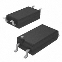
Optocoupler, Phototransistor Output,
SOP-4L, Long Mini-Flat Package
C
E
FEATURES
4
3
• SMD low profile 4 lead package
• VIORM = 1050 V
• CTR flexibility available see order information
• Special construction
1
A
17295-5
2
• Extra low coupling capacitance
C
• DC input with transistor output
• Creepage distance > 8 mm
• Material categorization:
for definitions of compliance please see
www.vishay.com/doc?99912
DESCRIPTION
The TCLT100. series consists of a phototransistor optically
coupled to a gallium arsenide infrared-emitting diode in a
4-lead SOP4L package.
AGENCY APPROVALS
• UL1577, file no. E76222
• CSA (cUL) 22.2 bulletin 5A recognized file no. E-76222
APPLICATIONS
• Switchmode power supplies
• BSI: BS EN 41003, BS EN 60065 (BS 415), BS EN 60950
(BS 7002), certificate number 7081 and 7402
• Computer peripheral interface
• DIN EN 60747-5-5 (VDE 0884)
• Microprocessor system interface
• FIMKO: EN 60950
• CQC
Note
• See the safety standard approval list “Agency Table” for more
detailed information.
ORDERING INFORMATION
T
C
L
T
1
0
0
SOP-4L
#
10.2 mm
PART NUMBER
AGENCY
CERTIFIED/PACKAGE
CTR (%)
5 mA
UL, cUL, VDE, BSI, FIMKO 50 to 600
SOP-4L
10 mA
5 mA
63 to 125 100 to 200 160 to 320 50 to 150 100 to 300 80 to 160 130 to 260 200 to 400
TCLT1000 TCLT1002 TCLT1003 TCLT1004 TCLT1005 TCLT1006 TCLT1007 TCLT1008 TCLT1009
Note
• Available only on tape and reel.
Document Number: 83515
1
For technical questions, contact: optocoupleranswers@vishay.com
THIS DOCUMENT IS SUBJECT TO CHANGE WITHOUT NOTICE. THE PRODUCTS DESCRIBED HEREIN AND THIS DOCUMENT
ARE SUBJECT TO SPECIFIC DISCLAIMERS, SET FORTH AT www.vishay.com/doc?91000
Rev. 2.9, 01-Dec-15
�TCLT100. Series
www.vishay.com
Vishay Semiconductors
ABSOLUTE MAXIMUM RATINGS (Tamb = 25 °C, unless otherwise specified)
PARAMETER
CONDITION
SYMBOL
VALUE
UNIT
INPUT
Reverse voltage
VR
6
V
Forward current
IF
60
mA
Forward surge current
tp ≤ 10 μs
IFSM
1.5
A
Pdiss
100
mW
Tj
125
°C
Collector emitter voltage
VCEO
70
V
Emitter collector voltage
VECO
7
V
mA
Power dissipation
Junction temperature
OUTPUT
Collector current
Collector peak current
tp/T = 0.5, tp ≤ 10 ms
Power dissipation
Junction temperature
IC
50
ICM
100
mA
Pdiss
150
mW
Tj
125
°C
COUPLER
Total power dissipation
Ptot
250
mW
Operating ambient temperature range
Tamb
-55 to +100
°C
Storage temperature range
Tstg
-55 to +125
°C
Soldering temperature
Tsld
260
°C
Note
• Stresses in excess of the absolute maximum ratings can cause permanent damage to the device. Functional operation of the device is not
implied at these or any other conditions in excess of those given in the operational sections of this document. Exposure to absolute
maximum ratings for extended periods of the time can adversely affect reliability.
ELECTRICAL CHARACTERISTICS (Tamb = 25 °C, unless otherwise specified)
PARAMETER
TEST CONDITION
SYMBOL
MIN.
TYP.
MAX.
UNIT
INPUT
Forward voltage
IF = 50 mA
VF
-
1.25
1.6
V
VR = 0 V, f = 1 MHz
Cj
-
50
-
pF
Collector emitter voltage
IC = 1 mA
VCEO
70
-
-
V
Emitter collector voltage
IE = 100 μA
VECO
7
-
-
V
VCE = 20 V, IF = 0 A
ICEO
-
10
100
nA
Collector emitter saturation voltage
IF = 10 mA, IC = 1 mA
VCEsat
-
-
0.3
V
Cut-off frequency
VCE = 5 V, IF = 10 mA,
RL = 100 Ω
fc
-
110
-
kHz
f = 1 MHz
Ck
-
0.3
-
pF
Junction capacitance
OUTPUT
Collector emitter cut-off current
COUPLER
Coupling capacitance
Note
• Minimum and maximum values are testing requirements. Typical values are characteristics of the device and are the result of engineering
evaluation. Typical values are for information only and are not part of the testing requirements.
Document Number: 83515
2
For technical questions, contact: optocoupleranswers@vishay.com
THIS DOCUMENT IS SUBJECT TO CHANGE WITHOUT NOTICE. THE PRODUCTS DESCRIBED HEREIN AND THIS DOCUMENT
ARE SUBJECT TO SPECIFIC DISCLAIMERS, SET FORTH AT www.vishay.com/doc?91000
Rev. 2.9, 01-Dec-15
�TCLT100. Series
www.vishay.com
Vishay Semiconductors
CURRENT TRANSFER RATIO (Tamb = 25 °C, unless otherwise specified)
PARAMETER
TEST CONDITION
PART
SYMBOL
MIN.
TYP.
MAX.
UNIT
VCE = 5 V, IF = 5 mA
TCLT1000
CTR
50
-
600
%
TCLT1002
CTR
63
-
125
%
TCLT1003
CTR
100
-
200
%
TCLT1004
CTR
160
-
320
%
TCLT1002
CTR
22
45
-
%
TCLT1003
CTR
34
70
-
%
TCLT1004
CTR
56
100
-
%
TCLT1005
CTR
50
-
150
%
TCLT1006
CTR
100
-
300
%
TCLT1007
CTR
80
-
160
%
TCLT1008
CTR
130
-
260
%
TCLT1009
CTR
200
-
400
%
VCE = 5 V, IF = 10 mA
VCE = 5 V, IF = 1 mA
IC/IF
VCE = 5 V, IF = 5 mA
SAFETY AND INSULATION RATINGS
PARAMETER
Partial discharge test voltage - routine test
Partial discharge test voltage lot test (sample test)
CONDITION
SYMBOL
VALUE
100 %, ttest = 1 s
Vpd
2
kV
tTr = 60 s, ttest = 10 s,
(see figure 2)
VIOTM
8
kVpeak
Vpd
1.68
kVpeak
VISO
5000
VRMS
VIO = 500 V
RIO
1012
Ω
VIO = 500 V, Tamb = 100 °C
RIO
1011
Ω
RIO
109
Ω
Isolation test voltage (RMS)
Insulation resistance
UNIT
VIO = 500 V, Tamb = 150 °C
(construction test only)
Forward current
Isi
130
mA
Pso
265
mW
VIOTM
8
kV
Safety temperature
Tsi
150
°C
Comparative tracking index
CTI
175
Power dissipation
Rated impulse voltage
Clearance distance
8.0
mm
Creepage distance
8.0
mm
Insulation distance (internal)
0.40
mm
Note
• According to DIN EN 60747-5-2 (VDE 0884) (see figure 2). This optocoupler is suitable for safe electrical isolation only within the safety
ratings. Compliance with the safety ratings shall be ensured by means of suitable protective circuits.
VIOTM
300
t1, t2
t3 , t4
ttest
tstres
Phototransistor
Pso (mW)
250
200
= 1 s to 10 s
=1s
= 10 s
= 12 s
Vpd
150
VIOWM
VIORM
100
IR-diode
Isi (mA)
50
0
0
0
94 9182-2
25
50
75
100
125
Tsi - Safety Temperature (°C)
Fig. 1 - Derating Diagram
150
13930
t3 ttest t4
t1
tTr = 60 s
t2
t stres
t
Fig. 2 - Test Pulse Diagram for Sample Test according to
DIN EN 60747-5-2 (VDE 0884); IEC60747-5-5
Document Number: 83515
3
For technical questions, contact: optocoupleranswers@vishay.com
THIS DOCUMENT IS SUBJECT TO CHANGE WITHOUT NOTICE. THE PRODUCTS DESCRIBED HEREIN AND THIS DOCUMENT
ARE SUBJECT TO SPECIFIC DISCLAIMERS, SET FORTH AT www.vishay.com/doc?91000
Rev. 2.9, 01-Dec-15
�TCLT100. Series
www.vishay.com
Vishay Semiconductors
SWITCHING CHARACTERISTICS (Tamb = 25 °C, unless otherwise specified)
PARAMETER
TEST CONDITION
SYMBOL
MIN.
TYP.
MAX.
UNIT
Delay time
VS = 5 V, IC = 2 mA, RL = 100 Ω,
(see figure 3)
td
-
3
-
μs
Rise time
VS = 5 V, IC = 2 mA, RL = 100 Ω,
(see figure 3)
tr
-
3
-
μs
Fall time
VS = 5 V, IC = 2 mA, RL = 100 Ω,
(see figure 3)
tf
-
4.7
-
μs
Storage time
VS = 5 V, IC = 2 mA, RL = 100 Ω,
(see figure 3)
ts
-
0.3
-
μs
Turn-on time
VS = 5 V, IC = 2 mA, RL = 100 Ω,
(see figure 3)
ton
-
6
-
μs
Turn-off time
VS = 5 V, IC = 2 mA, RL = 100 Ω,
(see figure 3)
toff
-
5
-
μs
Turn-on time
VS = 5 V, IF = 10 mA, RL = 1 kΩ,
(see figure 4)
ton
-
9
-
μs
Turn-off time
VS = 5 V, IF = 10 mA, RL = 1 kΩ,
(see figure 4)
toff
-
10
-
μs
IF
IF
0
+5V
IF
0
I C = 2 mA; adjusted through
input amplitude
tp
IC
t
100 %
90 %
R G = 50 Ω
tp
= 0.01
T
t p = 50 µs
Channel I
Channel II
50 Ω
Oscilloscope
R L = 1 MΩ
C L = 20 pF
10 %
0
tr
td
t on
100 Ω
tp
td
tr
t on (= td + tr)
95 10804
Fig. 3 - Test Circuit, Non-Saturated Operation
IF
Pulse duration
Delay time
Rise time
Turn-on time
ts
tf
t off
ts
tf
t off (= ts + tf)
t
Storage time
Fall time
Turn-off time
96 11698
Fig. 5 - Switching Times
+5V
I F = 10 mA
0
IC
R G = 50 Ω
tp
= 0.01
T
t p = 50 µs
Channel I
Channel II
50 Ω
Oscilloscope
R L ≥ 1 MΩ
C L ≤ 20 pF
1 kΩ
95 10843
Fig. 4 - Test Circuit, Saturated Operation
Document Number: 83515
4
For technical questions, contact: optocoupleranswers@vishay.com
THIS DOCUMENT IS SUBJECT TO CHANGE WITHOUT NOTICE. THE PRODUCTS DESCRIBED HEREIN AND THIS DOCUMENT
ARE SUBJECT TO SPECIFIC DISCLAIMERS, SET FORTH AT www.vishay.com/doc?91000
Rev. 2.9, 01-Dec-15
�TCLT100. Series
www.vishay.com
Vishay Semiconductors
1.2
300
NCTR - Normalized CTR (sat)
Ptot - Total Power Dissipation (mW)
TYPICAL CHARACTERISTICS (Tamb = 25 °C, unless otherwise specified)
Coupled device
250
200
Phototransistor
150
IR-diode
100
50
0
40
0.6
0.4
0.2
Normalized to CTR value:
IF = 5 mA, VCE = 5 V, Tamb = 25 °C
80
-60 -40 -20
120
Tamb - Ambient Temperature (°C)
96 11700
40
60
80 100 120
1.4
NCTR - Normalized CTR (NS)
Tamb = 110 °C
Tamb = 75 °C
Tamb = 25 °C
Tamb = 0 °C
Tamb = - 55 °C
1
0.1
Tamb = 0 °C
1.2
Tamb = -55 °C
Tamb = 25 °C
1.0
0.8
0.6
Tamb = 75 °C
0.4
Tamb = 100 °C
0.2
Normalized to:
IF = 5 mA, VCE = 5 V
0
0.6
0.8
1.0
1.2
1.4
1.6
0.1
VF - Forward Voltage (V)
Fig. 7 - Forward Current vs. Forward Voltage
1
10
100
IF - Forward Current (mA)
Fig. 10 - Normalized Current Transfer Ratio (non-saturated) vs.
Forward Current
1.2
1.2
IF = 5 mA
1.0
0.8
0.6
0.4
Normalized to CTR value:
IF = 5 mA, VCE = 5 V, Tamb = 25 °C
0
-60 -40 -20
0
20
40
60
80 100 120
Tamb - Ambient Temperature (°C)
Fig. 8 - Normalized Current Transfer Ratio (non-saturated) vs.
Ambient Temperature
NCTR - Normalized CTR (sat)
NCTR - Normalized CTR (non-saturated)
20
Fig. 9 - Normalized Current Transfer Ratio (saturated) vs.
Ambient Temperature
100
0.2
0
Tamb - Ambient Temperature (°C)
Fig. 6 - Total Power Dissipation vs. Ambient Temperature
IF - Forward Current (mA)
0.8
0
0
10
1.0
1.0
0.8
VCE = 0.4 V
Normalized to:
IF = 5 mA,
VCE = 5 V,
Tamb = 25 °C
Tamb = 0 °C
Tamb = -55
- °C
0.6
0.4
Tamb = 25 °C
0.2
Tamb = 75 °C
Tamb = 100 °C
0
0.1
1
10
100
IF - Forward Current (mA)
Fig. 11 - Normalized Current Transfer Ratio (saturated) vs.
Forward Current
Document Number: 83515
5
For technical questions, contact: optocoupleranswers@vishay.com
THIS DOCUMENT IS SUBJECT TO CHANGE WITHOUT NOTICE. THE PRODUCTS DESCRIBED HEREIN AND THIS DOCUMENT
ARE SUBJECT TO SPECIFIC DISCLAIMERS, SET FORTH AT www.vishay.com/doc?91000
Rev. 2.9, 01-Dec-15
�TCLT100. Series
www.vishay.com
Vishay Semiconductors
10 000
1.0
20 % used
VCEsat - Collector Emitter
Saturation Voltage (V)
ICE0 - Leakage Current (nA)
IF = 0 mA
1000
VCE = 40 V
100
10
VCE = 24 V
1
0.1
VCE = 12 V
0.01
0.8
CTR = 50 %
used
0.6
0.4
0.2
10 % used
0.001
0
-60 -40 -20
0
20
40
60
80 100 120
Fig. 12 - Collector Dark Current vs. Ambient Temperature
VCE = 5 V
10
1
0.1
1
100
10
IF - Forward Current (mA)
95 11027
20 mA
IF = 50 mA
10 mA
5 mA
2 mA
1
1 mA
0.1
0.1
95 10985
1
10
VCE = 5 V
100
10
1
0.1
1
10
8
Fig. 14 - Collector Current vs. Collector Emitter Voltage
Non-saturated
operation
VS = 5 V
RL = 100 Ω
ton
6
toff
4
2
0
100
VCE - Collector Emitter Voltage (V)
100
10
IF - Forward Current (mA)
Fig. 16 - Current Transfer Ratio vs. Forward Current
ton/toff - Turn-On/Turn-Off Time (µs)
IC - Collector Current (mA)
100
10
1000
95 11029
Fig. 13 - Collector Current vs. Forward Current
100
10
IC - Collector Current (mA)
Fig. 15 - Collector Emitter Saturation Voltage vs. Collector Current
CTR - Current Transfer Ratio (%)
IC - Collector Current (mA)
100
0.01
0.1
1
95 11028
Tamb - Ambient Temperature (°C)
0
95 11030
2
4
6
8
IC - Collector Current (mA)
Fig. 17 - Turn-on/off Time vs. Collector Current
Document Number: 83515
6
For technical questions, contact: optocoupleranswers@vishay.com
THIS DOCUMENT IS SUBJECT TO CHANGE WITHOUT NOTICE. THE PRODUCTS DESCRIBED HEREIN AND THIS DOCUMENT
ARE SUBJECT TO SPECIFIC DISCLAIMERS, SET FORTH AT www.vishay.com/doc?91000
Rev. 2.9, 01-Dec-15
�TCLT100. Series
ton/toff - Turn-On/Turn-Off Time (µs)
www.vishay.com
Vishay Semiconductors
50
Saturated operation
VS = 5 V
RL = 1 kΩ
40
30
toff
20
10
ton
0
5
0
10
15
20
IF - Forward Current (mA)
95 11031
Fig. 18 - Turn-on/off Time vs. Forward Current
PACKAGE DIMENSIONS (in millimeters)
2.30 max.
4.10 max.
10.20
3.80
+ 0.30
- 0.40
0.20
2.00
+ 0.10
- 0.05
7.50 ± 0.20
0.10
Seating plane
0.45 ± 0.1
0.70
+ 0.30
- 0.40
2.54 nom.
4
3
2.54
Possible footprint
0.90
8.20
1
22533
10.80
technical drawings
according to DIN
specifications
2
Pin no. 1 identification
PACKAGE MARKING (example)
TCLT1003
V YWW 68
Document Number: 83515
7
For technical questions, contact: optocoupleranswers@vishay.com
THIS DOCUMENT IS SUBJECT TO CHANGE WITHOUT NOTICE. THE PRODUCTS DESCRIBED HEREIN AND THIS DOCUMENT
ARE SUBJECT TO SPECIFIC DISCLAIMERS, SET FORTH AT www.vishay.com/doc?91000
Rev. 2.9, 01-Dec-15
�TCLT100. Series
www.vishay.com
Vishay Semiconductors
TAPE AND REEL DIMENSIONS (in millimeters)
Ø 1.55
2.7
4
2
0.3
7.5
Tape slot
in core
1.75
ESD sticker
10.6
16
330
(13")
5°
4.25
8
Ø 1.6
Regular, special
or bar code label
technical drawings
according to DIN
specification
17999
Fig. 19 - Reel Dimensions (3000 units per reel)
SOLDER PROFILE
22662
Fig. 20 - Tape Dimensions
HANDLING AND STORAGE CONDITIONS
ESD level: HBM class 2
300
max. 260 °C
245 °C
255 °C
240 °C
217 °C
250
Temperature (°C)
2.3
Direction of pulling out
Floor life: unlimited
Conditions: Tamb < 30 °C, RH < 85 %
Moisture sensitivity level 1, according to J-STD-020
200
max. 30 s
150
max. 100 s
max. 120 s
100
max. ramp down 6 °C/s
50
max. ramp up 3 °C/s
0
0
19841
50
100
150
200
250
300
Time (s)
Fig. 21 - Lead (Pb)-free Reflow Solder Profile
according to J-STD-020
Document Number: 83515
8
For technical questions, contact: optocoupleranswers@vishay.com
THIS DOCUMENT IS SUBJECT TO CHANGE WITHOUT NOTICE. THE PRODUCTS DESCRIBED HEREIN AND THIS DOCUMENT
ARE SUBJECT TO SPECIFIC DISCLAIMERS, SET FORTH AT www.vishay.com/doc?91000
Rev. 2.9, 01-Dec-15
�Legal Disclaimer Notice
www.vishay.com
Vishay
Disclaimer
ALL PRODUCT, PRODUCT SPECIFICATIONS AND DATA ARE SUBJECT TO CHANGE WITHOUT NOTICE TO IMPROVE
RELIABILITY, FUNCTION OR DESIGN OR OTHERWISE.
Vishay Intertechnology, Inc., its affiliates, agents, and employees, and all persons acting on its or their behalf (collectively,
“Vishay”), disclaim any and all liability for any errors, inaccuracies or incompleteness contained in any datasheet or in any other
disclosure relating to any product.
Vishay makes no warranty, representation or guarantee regarding the suitability of the products for any particular purpose or
the continuing production of any product. To the maximum extent permitted by applicable law, Vishay disclaims (i) any and all
liability arising out of the application or use of any product, (ii) any and all liability, including without limitation special,
consequential or incidental damages, and (iii) any and all implied warranties, including warranties of fitness for particular
purpose, non-infringement and merchantability.
Statements regarding the suitability of products for certain types of applications are based on Vishay's knowledge of typical
requirements that are often placed on Vishay products in generic applications. Such statements are not binding statements
about the suitability of products for a particular application. It is the customer's responsibility to validate that a particular product
with the properties described in the product specification is suitable for use in a particular application. Parameters provided in
datasheets and / or specifications may vary in different applications and performance may vary over time. All operating
parameters, including typical parameters, must be validated for each customer application by the customer's technical experts.
Product specifications do not expand or otherwise modify Vishay's terms and conditions of purchase, including but not limited
to the warranty expressed therein.
Hyperlinks included in this datasheet may direct users to third-party websites. These links are provided as a convenience and
for informational purposes only. Inclusion of these hyperlinks does not constitute an endorsement or an approval by Vishay of
any of the products, services or opinions of the corporation, organization or individual associated with the third-party website.
Vishay disclaims any and all liability and bears no responsibility for the accuracy, legality or content of the third-party website
or for that of subsequent links.
Except as expressly indicated in writing, Vishay products are not designed for use in medical, life-saving, or life-sustaining
applications or for any other application in which the failure of the Vishay product could result in personal injury or death.
Customers using or selling Vishay products not expressly indicated for use in such applications do so at their own risk. Please
contact authorized Vishay personnel to obtain written terms and conditions regarding products designed for such applications.
No license, express or implied, by estoppel or otherwise, to any intellectual property rights is granted by this document or by
any conduct of Vishay. Product names and markings noted herein may be trademarks of their respective owners.
© 2022 VISHAY INTERTECHNOLOGY, INC. ALL RIGHTS RESERVED
Revision: 01-Jan-2022
1
Document Number: 91000
�