TCND3000
Vishay Semiconductors
Reflective Sensor for Touchless Switch
FEATURES
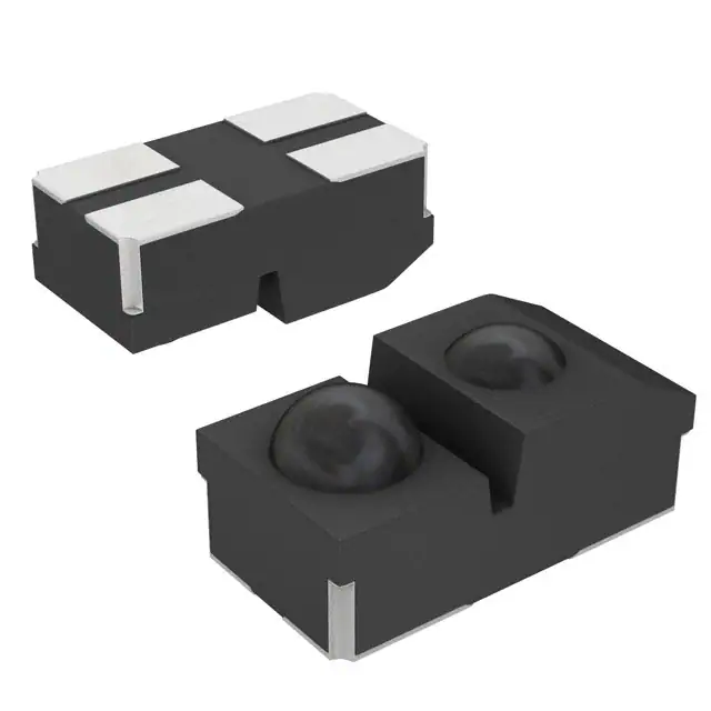
• Package type: surface mount
• Detector type: pin photodiode
• Dimensions (L x W x H in mm): 4.83 x 2.54 x 2.21
• Peak operating distance: 20 mm
• Peak operating range: 10 mm to 20 mm
• Typical output current under test: IC > 5.6 µA
84606 3D
• Lead (Pb)-free soldering released
• Compliant to RoHS directive 2002/95/EC
accordance to WEEE 2002/96/EC
DESCRIPTION
TCND3000 is a reflective optical sensor for applications
using the HALIOS® (High Ambient Light Independent Optical
System) principle. It consists of an infrared emitter and a
photodetector forming the optical sensing path. According to
the HALIOS principle a second infrared emitter is used for
compensation of disturbing ambient light. Optoelectronic
parameters of the sensor are matched to the corresponding
integrated circuit E909.01, manufactured by ELMOS
Semiconductor AG (www.elmos.de).
and
in
• Emitter wavelength: 885 nm
• Daylight blocking filter
• Touch distance: 10 mm (1)
• Proximity distance: 20 mm (1)
• High ambient light suppression for sunlight: ≤ 200 klx
• High ambient light suppression for CIE standard illuminant
A: ≤ 100 klx
Note
(1) Using E909.01 interface ASIC and Kodak grey card with 20 %
diffuse reflection
APPLICATIONS
• Optical switches for general purpose
PRODUCT SUMMARY
PART NUMBER
DISTANCE FOR
MAXIMUM CTRrel (1)
(mm)
TCND3000
0
DISTANCE RANGE FOR
TYPICAL OUTPUT
DAYLIGHT
RELATIVE Iout > 20 %
CURRENT UNDER TEST (2) BLOCKING FILTER
INTEGRATED
(mm)
(mA)
Not applicable
IC interface
Yes
Notes
(1) CTR: current transfere ratio, I /I
out in
(2) Conditions like in table basic charactristics/sensors
ORDERING INFORMATION
ORDERING CODE
PACKAGING
VOLUME (1)
REMARKS
TCND3000
Tape and reel
MOQ: 800 pcs, 800 pcs/reel
Drypack
Note
(1) MOQ: minimum order quantity
Document Number: 84606
Rev. 1.3, 13-May-09
For technical questions, contact: sensorstechsupport@vishay.com
www.vishay.com
1
�TCND3000
Reflective Sensor for Touchless
Switch
Vishay Semiconductors
ABSOLUTE MAXIMUM RATINGS
PARAMETER
(1)
TEST CONDITION
SYMBOL
VALUE
UNIT
mW
SENSOR
Tamb ≤ 25 °C
Power dissipation
PV
180
Storage temperature range
Tstg
- 40 to + 100
°C
Ambient temperature range
Tamb
- 40 to + 85
°C
Thermal resistance
junction/ambient
RthJA
450
K/W
Tsd
260
°C
VRS
5
V
IFS
50
mA
IFS
100
mA
TjS
105
°C
Soldering temperature
Acc. fig. 7
IR EMITTER LEDS (TRANSMITTER)
Reverse voltage
Forward current
Peak forward current
tps = 4 µs, tS = 8 µs
Junction temperature
IR EMITTER LEDC (COMPENSATION)
Reverse voltage
VRC
5
V
Forward current
IFC
50
mA
IFC
100
mA
TjC
105
°C
Peak forward current
tpc = 4 µs, tS = 8 µs
Junction temperature
DETECTOR
Reverse voltage
VRD
5
V
Junction temperature
TjD
105
°C
Note
(1) T
amb = 25 °C, unless otherwise specified
ABSOLUTE MAXIMUM RATINGS
PV - Power Dissipation (mW)
200
150
R thJA
100
50
0
0
84606Fig.2
20
40
60
80
100
Tamb - Ambient Temperature (°C)
Fig. 1 - Power Dissipation Limit vs. Ambient Temperature
BASIC CHARACTERISTICS
(1)
PARAMETER
TEST CONDITION
SYMBOL
Kodak grey card,
20 % diffuse reflection,
distance: 1 cm, IFS = 10 mA
ICA
1.2
no reflective medium, IFS = 10 mA
ICA
0.9
µA
IFC = 2 mA
ICR
5
µA
MIN.
TYP.
MAX.
UNIT
SENSOR
Light Current
Optical crosstalk sensing path
Compensation current
www.vishay.com
2
For technical questions, contact: sensorstechsupport@vishay.com
µA
Document Number: 84606
Rev. 1.3, 13-May-09
�TCND3000
Reflective Sensor for Touchless
Switch
BASIC CHARACTERISTICS
(1)
PARAMETER
TEST CONDITION
SYMBOL
Vishay Semiconductors
MIN.
TYP.
MAX.
UNIT
IR EMITTER LEDS (TRANSMITTER)
Forward voltage
IFS = 10 mA, tp = 20 ms
VFS
Reverse voltage
IRS = 10 µA
VRS
Junction capacitance
Radiant intensity
IFS = 10 mA, tp = 20 ms
Angle of half intensity
1.3
V
5
V
Cjs
50
Ie
2
ϕS
± 20
pF
22
mW/sr
deg
Peak wavelength
IFS = 10 mA
λpS
885
nm
Spectral bandwidth
IFS = 10 mA
ΔλS
42
nm
DIN EN ISO 1146/1:2005
d
1.4
mm
Virtual source diameter
875
IR EMITTER LEDC (COMPENSATION)
Forward voltage
IFC = 10 mA, tpC = 20 ms
VFC
Reverse voltage
IRC = 10 µA
VRC
CjC
50
pF
Peak wavelength
IFC = 10 mA
λpC
885
nm
Spectral bandwidth
IFC = 10 mA
ΔλC
42
nm
Junction capacitance
1.3
V
5
V
DETECTOR
Forward voltage
IFD = 50 mA
VFD
IRD = 100 µA, E = 0 lx
VBR
Reverse dark current
VRD = 10 V, E = 0 lx
Ir0
1
Reverse light current
Ee = 1 mW/cm2,
λ = 870 nm, VRD = 5 V
Ira
5.6
µA
Temperature coefficient of Ira
λ = 870 nm, VRD = 5 V
Breakdown voltage
1
1.3
V
5
V
10
nA
TKira
0.2
%/K
Angle of half intensity
ϕD
± 20
deg
Wavelength of peak sensitivity
λP
910
nm
Range of spectral bandwidth
λ0.5
790 to 1020
nm
Note
(1) T
amb = 25 °C, unless otherwise specified
BASIC CHARACTERISTICS
Tamb = 25 °C, unless otherwise specified
0°
10°
0°
20°
10°
20°
30°
0.9
50°
0.8
60°
70°
0.7
94 8883
Srel - Relative Intensity
40°
1.0
ϕ - Angular Displacement
Ie rel - Relative Radiant Intensity
30°
40°
1.0
0.9
50°
0.8
60°
70°
0.7
80°
80°
0.6
0.4
0.2
0
20181
Fig. 2 - Relative Radiant Intensity vs. Angular Displacement
Document Number: 84606
Rev. 1.3, 13-May-09
0.6
0.4
0.2
0
0.2
0.4
0.6
Fig. 3 - Relative Radiant Sensitivity vs. Angular Displacement
For technical questions, contact: sensorstechsupport@vishay.com
www.vishay.com
3
�TCND3000
Reflective Sensor for Touchless
Switch
1.2
3.5
1.0
ICA- Photocurrent (µA)
S( )rel - Relative Spectral Responsivity
Vishay Semiconductors
0.8
0.6
0.4
3
2.5
I FS = 10 mA
2
1.5
1
Crosstalk Level
0.2
0.5
0.0
600
84606Fig5_1
700
800
900
1000
0
1100
10
1
λ - Wavelength (nm)
84606Fig6_1
Fig. 4 - Relative Spectral Sensitivity vs. Wavelength
100
d - Distance (mm)
Fig. 5 - Photocurrent vs. Distance
APPLICATION CIRCUIT
TCND_3000_Fig.6
Fig. 6 - Test Circuit
www.vishay.com
4
For technical questions, contact: sensorstechsupport@vishay.com
Document Number: 84606
Rev. 1.3, 13-May-09
�TCND3000
Reflective Sensor for Touchless
Switch
Vishay Semiconductors
PACKAGE DIMENSIONS in millimeters
84606 Dimensions
Document Number: 84606
Rev. 1.3, 13-May-09
For technical questions, contact: sensorstechsupport@vishay.com
www.vishay.com
5
�TCND3000
Reflective Sensor for Touchless
Switch
Vishay Semiconductors
REFLOW SOLDER PROFILES
Temperature (°C)
Preheat
280
260
240
220
200
180
160
140
120
100
DRYPACK
Reflow
Devices are packed in moisture barrier bags (MBB) to
prevent the products from moisture absorption during
transportation and storage. Each bag contains a desiccant.
Cooling
FLOOR LIFE
260 °C
250 °C
Floor life (time between soldering and removing from MBB)
must not exceed the time indicated on MBB label:
Floor life: 4 weeks
Conditions: Tamb < 30 °C, RH < 60 %
Moisture sensitivity level 2a, acc. to J-STD-020.
210 °C
145 °C
125 °C
~ 20 s
80
60
40
20
0
60
30
0
90
DRYING
~ 30 s
~ 40 s
120 s
120
150
180
210
240
270
300
Time (s)
19030
In case of moisture absorption devices should be baked
before soldering. Conditions see J-STD-020 or label.
Devices taped on reel dry using recommended conditions
192 h at 40 °C (+ 5 °C), RH < 5 %.
Fig. 7 - Lead (Pb)-free Reflow Solder Profile acc. J-STD-020
948625
300
max. 240 °C
10 s
ca. 230 °C
Temperature (°C)
250
200
215 °C
150
max 40 s
max. 160 °C
100
90 s to 120 s
Lead Temperature
50
Full Line: Typical
Dotted: Process Limits
2 K/s to 4 K/s
0
0
50
100
150
200
250
Time (s)
Fig. 8 - Lead (Pb)-free Reflow Solder Profile acc. J-STD-020
www.vishay.com
6
For technical questions, contact: sensorstechsupport@vishay.com
Document Number: 84606
Rev. 1.3, 13-May-09
�Legal Disclaimer Notice
Vishay
Disclaimer
All product specifications and data are subject to change without notice.
Vishay Intertechnology, Inc., its affiliates, agents, and employees, and all persons acting on its or their behalf
(collectively, “Vishay”), disclaim any and all liability for any errors, inaccuracies or incompleteness contained herein
or in any other disclosure relating to any product.
Vishay disclaims any and all liability arising out of the use or application of any product described herein or of any
information provided herein to the maximum extent permitted by law. The product specifications do not expand or
otherwise modify Vishay’s terms and conditions of purchase, including but not limited to the warranty expressed
therein, which apply to these products.
No license, express or implied, by estoppel or otherwise, to any intellectual property rights is granted by this
document or by any conduct of Vishay.
The products shown herein are not designed for use in medical, life-saving, or life-sustaining applications unless
otherwise expressly indicated. Customers using or selling Vishay products not expressly indicated for use in such
applications do so entirely at their own risk and agree to fully indemnify Vishay for any damages arising or resulting
from such use or sale. Please contact authorized Vishay personnel to obtain written terms and conditions regarding
products designed for such applications.
Product names and markings noted herein may be trademarks of their respective owners.
Document Number: 91000
Revision: 18-Jul-08
www.vishay.com
1
�