TCND5000
www.vishay.com
Vishay Semiconductors
Reflective Optical Sensor with PIN Photodiode Output
FEATURES
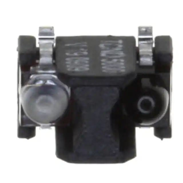
Top view
A
• Package type: surface mount
A
• Detector type: pin photodiode
• Dimensions (L x W x H in mm): 6 x 4.3 x 3.75
Detector
Emitter
C
19967
• Operating range within > 20 % relative collector
current: 2 mm to 25 mm
C
• Typical output current under test: Ira > 0.11 μA
Marking area
21846
• Peak operating distance: 6 mm
• Daylight blocking filter
DESCRIPTION
• High linearity
The TCND5000 is a reflective sensor that includes an
infrared emitter and pin photodiode in a surface mount
package which blocks visible light.
• Emitter wavelength: 940 nm
• Lead (Pb)-free soldering released
• Moisture sensitivity level (MSL): 4
• Material categorization: for definitions of compliance
please see www.vishay.com/doc?99912
APPLICATIONS
• Proximity sensor
• Object sensor
• Motion sensor
• Touch key
PRODUCT SUMMARY
PART NUMBER
DISTANCE FOR
MAXIMUM CTRrel (1)
(mm)
DISTANCE RANGE FOR
RELATIVE Iout > 20 %
(mm)
TYPICAL OUTPUT
CURRENT UNDER TEST (2)
(mA)
DAYLIGHT
BLOCKING FILTER
INTEGRATED
6
2 to 25
0.0015
Yes
TCND5000
Notes
(1) CTR: current transfer ratio, I /I
out in
(2) Conditions like in table basic characteristics/sensors
ORDERING INFORMATION
ORDERING CODE
PACKAGING
VOLUME
REMARKS
TCND5000
Tape and reel
MOQ: 2000 pcs, 2000 pcs/reel
Drypack
Note
• MOQ: minimum order quantity
ABSOLUTE MAXIMUM RATINGS (Tamb = 25 °C, unless otherwise specified)
PARAMETER
TEST CONDITION
SYMBOL
VALUE
UNIT
INPUT (EMITTER)
Reverse voltage
VR
5
V
Forward current
IF
100
mA
IFM
500
mA
Power dissipation
PV
190
mW
Junction temperature
Tj
100
°C
Peak forward current
Rev. 1.6, 12-Jun-14
tp = 50 μs, t = 2 ms, Tamb 25 °C
Document Number: 83795
1
For technical questions, contact: sensorstechsupport@vishay.com
THIS DOCUMENT IS SUBJECT TO CHANGE WITHOUT NOTICE. THE PRODUCTS DESCRIBED HEREIN AND THIS DOCUMENT
ARE SUBJECT TO SPECIFIC DISCLAIMERS, SET FORTH AT www.vishay.com/doc?91000
�TCND5000
www.vishay.com
Vishay Semiconductors
ABSOLUTE MAXIMUM RATINGS (Tamb = 25 °C, unless otherwise specified)
PARAMETER
TEST CONDITION
SYMBOL
VALUE
UNIT
Reverse voltage
VR
60
V
Power dissipation
PV
75
mW
Junction temperature
Tj
100
°C
OUTPUT (DETECTOR)
SENSOR
Ambient temperature range
Tamb
-40 to +85
°C
Storage temperature range
Tstg
-40 to +100
°C
Tsd
260
°C
Soldering temperature
acc. fig. 14
120
IF - Forward Current (mA)
100
80
60
40
20
0
0
16188
10 20 30 40 50 60 70 80 90 100
Tamb - Ambient Temperature (°C)
Fig. 1 - Forward Current Limit vs. Ambient Temperature
BASIC CHARACTERISTICS (Tamb = 25 °C, unless otherwise specified)
PARAMETER
TEST CONDITION
SYMBOL
MIN.
TYP.
MAX.
1.5
UNIT
INPUT (EMITTER) (1)
Forward voltage
Temperature coefficient of VF
Reverse current
IF = 50 mA, tp = 20 ms
VF
1.2
IF = 1 mA
TKVF
-1.3
V
mV/K
VR = 5 V
IR
VR = 0 V, f = 1 MHz, E = 0 lx
Cj
40
IF = 20 mA, tp = 20 ms
Ie
11
Peak wavelength
IF = 100 mA
P
Spectral bandwidth
IF = 100 mA
30
nm
Temperature coefficient of p
IF = 100 mA
TKP
0.2
nm/K
Rise time
IF = 100 mA
tr
15
ns
Fall time
IF = 100 mA
tf
15
ns
Junction capacitance
Radiant intensity
Angle of half intensity
Rev. 1.6, 12-Jun-14
930
10
μA
15
mW/sr
pF
± 12
deg
940
nm
Document Number: 83795
2
For technical questions, contact: sensorstechsupport@vishay.com
THIS DOCUMENT IS SUBJECT TO CHANGE WITHOUT NOTICE. THE PRODUCTS DESCRIBED HEREIN AND THIS DOCUMENT
ARE SUBJECT TO SPECIFIC DISCLAIMERS, SET FORTH AT www.vishay.com/doc?91000
�TCND5000
www.vishay.com
Vishay Semiconductors
BASIC CHARACTERISTICS (Tamb = 25 °C, unless otherwise specified)
PARAMETER
TEST CONDITION
SYMBOL
MIN.
TYP.
MAX.
UNIT
1
1.3
V
10
nA
OUTPUT (DETECTOR) (2)
Forward voltage
IF = 50 mA
VF
Breakdown voltage
IR = 100 μA
VBR
VR = 10 V, E = 0 lx
Iro
1
VR = 5 V, f = 1 MHz, E = 0 lx
CD
1.8
Reverse dark current
Diode capacitance
Reverse light current
mW/cm2,
Ee = 1
= 950 nm, VR = 5 V
60
V
pF
Ira
12
μA
TKira
0.2
%/K
Angle of half intensity
± 15
deg
Wavelength of peak sensitivity
P
930
nm
Range of spectral bandwidth
0.5
840 to 1050
nm
260
nA
= 870 nm, VR = 5 V
Temperature coefficient of Ira
SENSOR
VR = 2.5 V, IF = 20 mA, D = 30 mm,
reflective mode: see figure 2
Reverse Light Current
Ira
110
Notes
(1) See figures 2 to 8 accordingly
(2) See figures 9 to 12 accordingly
D = 30 mm
d = 26.25 mm
30 mm
Kodak grey card
20 % Reflectivity
18223
Fig. 2 - Test Circuit
BASIC CHARACTERISTICS (Tamb = 25 °C, unless otherwise specified)
1000
Ie - Radiant Intensity (mW/sr)
IF - Forward Current (mA)
1000
100
10
tp = 100 µs
tp/T= 0.001
tp = 100 μs
100
10
1
0.1
1
0
21534
1
2
VF - Forward Voltage (V)
Fig. 3 - Forward Current vs. Forward Voltage
Rev. 1.6, 12-Jun-14
3
1
10
100
1000
IF - Forward Current (mA)
Fig. 4 - Radiant Intensity vs. Forward Current
Document Number: 83795
3
For technical questions, contact: sensorstechsupport@vishay.com
THIS DOCUMENT IS SUBJECT TO CHANGE WITHOUT NOTICE. THE PRODUCTS DESCRIBED HEREIN AND THIS DOCUMENT
ARE SUBJECT TO SPECIFIC DISCLAIMERS, SET FORTH AT www.vishay.com/doc?91000
�TCND5000
www.vishay.com
Vishay Semiconductors
90
IF = 30 mA
80
70
60
50
40
30
20
10
0
840
880
920
960
1000
10°
1.0
0.8
0.6
0
0.9
50°
0.8
60°
0.7
70°
80°
0
18234
VCE = 5 V
λ = 950 nm
1.0
0.1
0.01
16055
Fig. 6 - Relative Radiant Intensity vs. Angular Displacement
0.1
1
10
Ee - Irradiance (mW/cm²)
Fig. 9 - Reverse Light Current vs. Irradiance
1000
8
CD - Diode Capacitance (pF)
Iro - Reverse Dark Current (nA)
10
0.6
0.4
0.2
100
100
Ira - Reverse Light Current (µA)
Ie rel - Relative Intensity
40°
0.2
80
60
20°
1.0
0.4
40
Fig. 8 - Relative Reverse Light Current vs. Ambient Temperature
30°
0.6
20
Tamb - Ambient Temperature (°C)
94 8416
Fig. 5 - Relative Radiant Power vs. Wavelength
0°
VR = 5 V
λ = 950 nm
1.2
1040
λ - Wavelength (nm)
21445
1.4
Ira, rel - Relative Reverse Light Current
Φe rel - Relative Radiant Power (%)
100
100
10
VR = 10 V
1
6
E=0
f = 1 MHz
4
2
0
20
94 8427
40
60
80
100
Tamb - Ambient Temperature (°C)
Fig. 7 - Reverse Dark Current vs. Ambient Temperature
Rev. 1.6, 12-Jun-14
0.1
94 8430
1
10
100
VR- Reverse Voltage (V)
Fig. 10 - Diode Capacitance vs. Reverse Voltage
Document Number: 83795
4
For technical questions, contact: sensorstechsupport@vishay.com
THIS DOCUMENT IS SUBJECT TO CHANGE WITHOUT NOTICE. THE PRODUCTS DESCRIBED HEREIN AND THIS DOCUMENT
ARE SUBJECT TO SPECIFIC DISCLAIMERS, SET FORTH AT www.vishay.com/doc?91000
�TCND5000
www.vishay.com
Vishay Semiconductors
S (λ) rel - Relative Spectral Sensitivity
1.2
1.0
0.8
0.6
0.4
0.2
0
750
850
950
1050
1150
λ - Wavelength (nm)
12786
Fig. 11 - Relative Spectral Sensitivity vs. Wavelength
0°
10°
20°
40°
1.0
0.9
50°
0.8
60°
70°
0.7
ϕ - Angular Displacement
Srel - Relative Sensitivity
30°
80°
0.6
0.4
0.2
0
94 8248
Fig. 12 - Relative Radiant Sensitivity vs. Angular Displacement
Ira, rel - Rel. Reverse Light Current
1.0
Media: Kodak Gray Card
IF = 10 mA
0.8
0.6
0.4
0.2
0.0
0
19966
5
10 15 20 25 30 35 40 45 50
d - Distance to Reflecting Card (mm)
Fig. 13 - Relative Reverse Light Current vs. Distance
Rev. 1.6, 12-Jun-14
Document Number: 83795
5
For technical questions, contact: sensorstechsupport@vishay.com
THIS DOCUMENT IS SUBJECT TO CHANGE WITHOUT NOTICE. THE PRODUCTS DESCRIBED HEREIN AND THIS DOCUMENT
ARE SUBJECT TO SPECIFIC DISCLAIMERS, SET FORTH AT www.vishay.com/doc?91000
�TCND5000
www.vishay.com
Vishay Semiconductors
TAPING DIMENSIONS in millimeters
18222
Rev. 1.6, 12-Jun-14
Document Number: 83795
6
For technical questions, contact: sensorstechsupport@vishay.com
THIS DOCUMENT IS SUBJECT TO CHANGE WITHOUT NOTICE. THE PRODUCTS DESCRIBED HEREIN AND THIS DOCUMENT
ARE SUBJECT TO SPECIFIC DISCLAIMERS, SET FORTH AT www.vishay.com/doc?91000
�TCND5000
www.vishay.com
Vishay Semiconductors
PACKAGE DIMENSIONS in millimeters
19968
Rev. 1.6, 12-Jun-14
Document Number: 83795
7
For technical questions, contact: sensorstechsupport@vishay.com
THIS DOCUMENT IS SUBJECT TO CHANGE WITHOUT NOTICE. THE PRODUCTS DESCRIBED HEREIN AND THIS DOCUMENT
ARE SUBJECT TO SPECIFIC DISCLAIMERS, SET FORTH AT www.vishay.com/doc?91000
�TCND5000
www.vishay.com
PRECAUTIONS FOR USE
Vishay Semiconductors
REFLOW SOLDER PROFILES
1. Over-current-proof
2.1 Storage temperature and rel. humidity conditions are:
5 °C to 30 °C, RH 60 %
2.2 Floor life must not exceed 72 h, acc. to JEDEC® level 4,
J-STD-020.
Once the package is opened, the products should be
used within 72 h. Otherwise, they should be kept in a
damp proof box with desiccant.
Considering tape life, we suggest to use products within
one year from production date.
max. 260 °C
245 °C
255 °C
250
Temperature (°C)
2. Storage
19003
300
Customer must apply resistors for protection, otherwise
slight voltage shift will cause big current change (Burn out
will happen).
240 °C
217 °C
200
max. 20 s
150
max. 120 s
max. 100 s
100
max. Ramp up 3°C/s
50
max. Ramp down 6°C/s
0
0
50
100
250
200
150
300
Time (s)
2.3 If opened more than 72 h in an atmosphere 5 °C to
30 °C, RH 60 %, devices should be treated at 60 °C ±
5 °C for 15 h.
Fig. 14 - Lead (Pb)-Free Reflow Solder Profile
2.4 If humidity indicator in the package shows pink color
(normal blue), then devices should be treated with the
same conditions as 2.3
948625
300
max. 240 °C
10 s
ca. 230 °C
Temperature (°C)
250
200
215 °C
150
max 40 s
max. 160 °C
100
90 s to 120 s
Lead Temperature
50
Full Line: Typical
Dotted: Process Limits
2 K/s to 4 K/s
0
0
50
100
150
200
250
Time (s)
Fig. 15 - Lead Tin (SnPb) Reflow Solder Profile
Rev. 1.6, 12-Jun-14
Document Number: 83795
8
For technical questions, contact: sensorstechsupport@vishay.com
THIS DOCUMENT IS SUBJECT TO CHANGE WITHOUT NOTICE. THE PRODUCTS DESCRIBED HEREIN AND THIS DOCUMENT
ARE SUBJECT TO SPECIFIC DISCLAIMERS, SET FORTH AT www.vishay.com/doc?91000
�Packaging and Ordering Information
Vishay Semiconductors
Packaging and Ordering Information
PART NUMBER
MOQ (1)
PCS PER TUBE
TUBE SPEC.
(FIGURE)
CONSTITUENTS
(FORMS)
CNY70
4000
80
1
28
TCPT1300X01
2000
Reel
(2)
29
TCRT1000
1000
Bulk
-
26
TCRT1010
1000
Bulk
-
26
TCRT5000
4500
50
2
27
TCRT5000L
2400
48
3
27
TCST1030
5200
65
5
24
TCST1030L
2600
65
6
24
TCST1103
1020
85
4
24
TCST1202
1020
85
4
24
TCST1230
4800
60
7
24
TCST1300
1020
85
4
24
TCST2103
1020
85
4
24
TCST2202
1020
85
4
24
TCST2300
1020
85
4
24
TCST5250
4860
30
8
24
TCUT1300X01
2000
Reel
(2)
29
TCZT8020-PAER
2500
Bulk
-
22
Notes
(1) MOQ: minimum order quantity
(2) Please refer to datasheets
TUBE SPECIFICATION FIGURES
15198
Fig. 1
Document Number: 80112
Rev. 1.1, 02-Jul-09
For technical questions, contact: optocoupleranswers@vishay.com
www.vishay.com
1
�Packaging and Ordering Information
Vishay Semiconductors Packaging and Ordering Information
15210
Fig. 2
15201
Fig. 3
www.vishay.com
2
For technical questions, contact: optocoupleranswers@vishay.com
Document Number: 80112
Rev. 1.1, 02-Jul-09
�Packaging and Ordering Information
Packaging and Ordering Information Vishay Semiconductors
15199
Fig. 4
15202
Fig. 5
Document Number: 80112
Rev. 1.1, 02-Jul-09
For technical questions, contact: optocoupleranswers@vishay.com
www.vishay.com
3
�Packaging and Ordering Information
Vishay Semiconductors Packaging and Ordering Information
15196
Fig. 6
15195
Fig. 7
www.vishay.com
4
For technical questions, contact: optocoupleranswers@vishay.com
Document Number: 80112
Rev. 1.1, 02-Jul-09
�Packaging and Ordering Information
Packaging and Ordering Information Vishay Semiconductors
20257
Fig. 8
Document Number: 80112
Rev. 1.1, 02-Jul-09
For technical questions, contact: optocoupleranswers@vishay.com
www.vishay.com
5
�Legal Disclaimer Notice
www.vishay.com
Vishay
Disclaimer
ALL PRODUCT, PRODUCT SPECIFICATIONS AND DATA ARE SUBJECT TO CHANGE WITHOUT NOTICE TO IMPROVE
RELIABILITY, FUNCTION OR DESIGN OR OTHERWISE.
Vishay Intertechnology, Inc., its affiliates, agents, and employees, and all persons acting on its or their behalf (collectively,
“Vishay”), disclaim any and all liability for any errors, inaccuracies or incompleteness contained in any datasheet or in any other
disclosure relating to any product.
Vishay makes no warranty, representation or guarantee regarding the suitability of the products for any particular purpose or
the continuing production of any product. To the maximum extent permitted by applicable law, Vishay disclaims (i) any and all
liability arising out of the application or use of any product, (ii) any and all liability, including without limitation special,
consequential or incidental damages, and (iii) any and all implied warranties, including warranties of fitness for particular
purpose, non-infringement and merchantability.
Statements regarding the suitability of products for certain types of applications are based on Vishay's knowledge of typical
requirements that are often placed on Vishay products in generic applications. Such statements are not binding statements
about the suitability of products for a particular application. It is the customer's responsibility to validate that a particular product
with the properties described in the product specification is suitable for use in a particular application. Parameters provided in
datasheets and / or specifications may vary in different applications and performance may vary over time. All operating
parameters, including typical parameters, must be validated for each customer application by the customer's technical experts.
Product specifications do not expand or otherwise modify Vishay's terms and conditions of purchase, including but not limited
to the warranty expressed therein.
Hyperlinks included in this datasheet may direct users to third-party websites. These links are provided as a convenience and
for informational purposes only. Inclusion of these hyperlinks does not constitute an endorsement or an approval by Vishay of
any of the products, services or opinions of the corporation, organization or individual associated with the third-party website.
Vishay disclaims any and all liability and bears no responsibility for the accuracy, legality or content of the third-party website
or for that of subsequent links.
Except as expressly indicated in writing, Vishay products are not designed for use in medical, life-saving, or life-sustaining
applications or for any other application in which the failure of the Vishay product could result in personal injury or death.
Customers using or selling Vishay products not expressly indicated for use in such applications do so at their own risk. Please
contact authorized Vishay personnel to obtain written terms and conditions regarding products designed for such applications.
No license, express or implied, by estoppel or otherwise, to any intellectual property rights is granted by this document or by
any conduct of Vishay. Product names and markings noted herein may be trademarks of their respective owners.
© 2022 VISHAY INTERTECHNOLOGY, INC. ALL RIGHTS RESERVED
Revision: 01-Jan-2022
1
Document Number: 91000
�