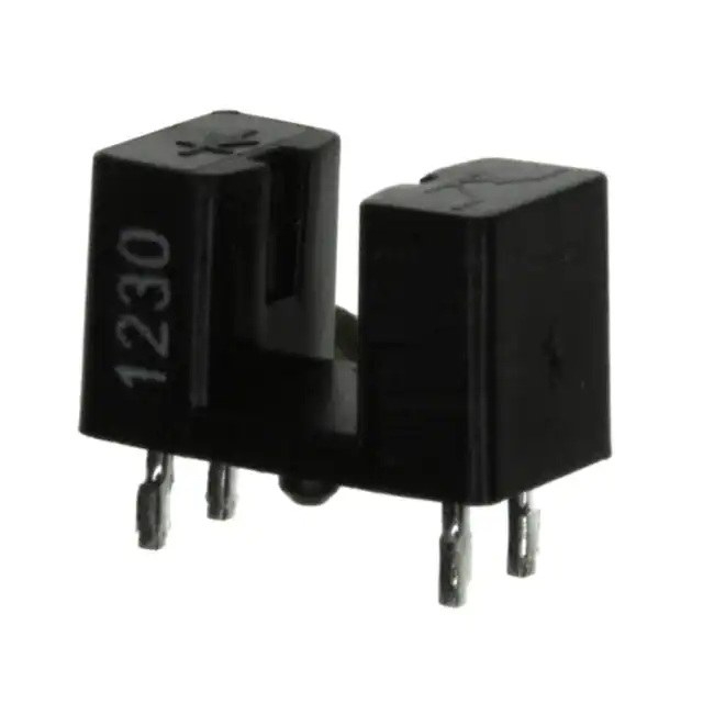
TCST1230
www.vishay.com
Vishay Semiconductors
Transmissive Optical Sensor with Phototransistor Output
FEATURES
• Package type: leaded
Top view
A
• Detector type: phototransistor
E
• Dimensions (L x W x H in mm): 9.2 x 4.8 x 5.4
• Gap (in mm): 2.8
C
• Aperture (in mm): 0.5
C
21833
• Typical output current under test: IC = 2 mA
19205_1
• Daylight blocking filter
• Emitter wavelength: 950 nm
DESCRIPTION
• Lead (Pb)-free soldering released
The TCST1230 is a transmissive sensor that includes an
infrared emitter and phototransistor, located face-to-face on
the optical axes in a leaded package which blocks visible
light.
• Material categorization: For definitions of compliance
please see www.vishay.com/doc?99912
APPLICATIONS
• Optical switch
• Shaft encoder
• Detection of opaque material such as paper
• Detection of magnetic tapes
PRODUCT SUMMARY
PART NUMBER
TCST1230
GAP WIDTH
(mm)
APERTURE WIDTH
(mm)
TYPICAL OUTPUT
CURRENT UNDER TEST (1)
(mA)
DAYLIGHT
BLOCKING FILTER
INTEGRATED
2.8
0.5
2
Yes
Note
• Conditions like in table basic characteristics/coupler
ORDERING INFORMATION
ORDERING CODE
TCST1230
PACKAGING
VOLUME (1)
REMARKS
Tube
MOQ: 4800 pcs, 60 pcs/tube
-
Note
• MOQ: minimum order quantity
ABSOLUTE MAXIMUM RATINGS (Tamb = 25 °C, unless otherwise specified)
PARAMETER
TEST CONDITION
SYMBOL
VALUE
UNIT
mW
COUPLER
Total power dissipation
Tamb ≤ 25 °C
Ptot
250
Ambient temperature range
Tamb
- 25 to + 85
°C
Storage temperature range
Tstg
- 40 to + 100
°C
Tsd
260
°C
Soldering temperature
Distance to package 1.6 mm, t ≤ 5 s
INPUT (EMITTER)
Reverse voltage
VR
6
V
Forward current
IF
60
mA
Forward surge current
Power dissipation
Junction temperature
tp ≤ 10 μs
IFSM
3
A
Tamb ≤ 25 °C
PV
100
mW
Tj
100
°C
Document Number: 83765
1
For technical questions, contact: sensorstechsupport@vishay.com
THIS DOCUMENT IS SUBJECT TO CHANGE WITHOUT NOTICE. THE PRODUCTS DESCRIBED HEREIN AND THIS DOCUMENT
ARE SUBJECT TO SPECIFIC DISCLAIMERS, SET FORTH AT www.vishay.com/doc?91000
Rev. 2.0, 21-Sep-12
�TCST1230
www.vishay.com
Vishay Semiconductors
ABSOLUTE MAXIMUM RATINGS (Tamb = 25 °C, unless otherwise specified)
PARAMETER
TEST CONDITION
SYMBOL
VALUE
UNIT
Collector emitter voltage
VCEO
70
V
Emitter collector voltage
VECO
7
V
OUTPUT (DETECTOR)
Collector current
Tamb ≤ 25 °C
Power dissipation
Junction temperature
IC
100
mA
PV
150
mW
Tj
100
°C
ABSOLUTE MAXIMUM RATINGS
P - Power Dissipation (mW)
400
300
Coupled device
200
Phototransistor
IR-diode
100
0
30
0
95 11088
60
90
120
150
Tamb - Ambient Temperature (°C)
Fig. 1 - Power Dissipation Limit vs. Ambient Temperature
BASIC CHARACTERISTICS (Tamb = 25 °C, unless otherwise specified)
PARAMETER
TEST CONDITION
SYMBOL
MIN.
Collector current
VCE = 10 V, IF = 20 mA
IC
0.5
Collector emitter saturation
voltage
IF = 20 mA, IC = 0.2 mA
VCEsat
TYP.
MAX.
UNIT
14
mA
0.4
V
COUPLER
INPUT (EMITTER)
Forward voltage
Junction capacitance
IF = 60 mA
VF
1.25
VR = 0 V, f = 1 MHz
Cj
50
IC = 1 mA
VCEO
70
7
1.5
V
pF
OUTPUT (DETECTOR)
Collector emitter voltage
Emitter collector voltage
V
IE = 10 μA
VECO
VCE = 25 V, IF = 0 A, E = 0 lx
ICEO
10
Turn-on time
IC = 1 mA, VCE = 5 V,
RL = 100 Ω (see figure 2)
ton
15
μs
Turn-off time
IC = 1 mA, VCE = 5 V,
RL = 100 Ω (see figure 2)
toff
10
μs
Collector dark current
V
100
nA
SWITCHING CHARACTERISTICS
Document Number: 83765
2
For technical questions, contact: sensorstechsupport@vishay.com
THIS DOCUMENT IS SUBJECT TO CHANGE WITHOUT NOTICE. THE PRODUCTS DESCRIBED HEREIN AND THIS DOCUMENT
ARE SUBJECT TO SPECIFIC DISCLAIMERS, SET FORTH AT www.vishay.com/doc?91000
Rev. 2.0, 21-Sep-12
�TCST1230
www.vishay.com
Vishay Semiconductors
IF
0
+5V
IF
IF
0
IC = 1 mA; adjusted by I F
tp
IC
t
100 %
90 %
RG = 50 Ω
tp
= 0.01
T
t p = 50 µs
Channel I
tr
R L ≥ 1 MΩ
CL ≤ 20 pF
Channel II
50 Ω
10 %
0
Oscilloscope
100 Ω
td
tp
td
tr
t on (= td + tr)
20223
ts
t on
ts
tf
t off (= ts + tf)
Pulse duration
Delay time
Rise time
Turn-on time
Fig. 2 - Test Circuit for ton and toff
t
tf
t off
Storage time
Fall time
Turn-off time
96 11698
Fig. 3 - Switching Times
BASIC CHARACTERISTICS (Tamb = 25 °C, unless otherwise specified)
10 000
ICEO - Collector Dark Current (nA)
IF - Forward Current (mA)
1000
100
10
1
100
10
1
0.1
0
0.4
0.8
1.2
1.6
2.0
VF - Forward Voltage (V)
96 11862
25
50
75
Tamb - Ambient Temperature (°C)
0
95 11090
Fig. 4 - Forward Current vs. Forward Voltage
100
Fig. 6 - Collector Dark Current vs. Ambient Temperature
10
2.0
VCE = 10 V
VCE = 5 V
I F = 20 mA
I C - Collector Current (mA)
CTR rel - Relative Current Transfer Ratio
VCE = 25 V
IF = 0 A
1000
1.5
1.0
0.5
0
- 25
95 11089
0
25
50
75
100
Tamb - Ambient Temperature (°C)
Fig. 5 - Relative Current Transfer Ratio vs. Ambient Temperature
1
0.1
0.01
0.001
0.1
95 11083
1
10
100
I F - Forward Current (mA)
Fig. 7 - Collector Current vs. Forward Current
Document Number: 83765
3
For technical questions, contact: sensorstechsupport@vishay.com
THIS DOCUMENT IS SUBJECT TO CHANGE WITHOUT NOTICE. THE PRODUCTS DESCRIBED HEREIN AND THIS DOCUMENT
ARE SUBJECT TO SPECIFIC DISCLAIMERS, SET FORTH AT www.vishay.com/doc?91000
Rev. 2.0, 21-Sep-12
�TCST1230
www.vishay.com
Vishay Semiconductors
110
I Crel - Relative Collector Current
I C - Collector Current (mA)
10
I F = 50 mA
1
20 mA
10 mA
0.1
5 mA
2 mA
0.01
0.1
1
10
100
VCE - Collector Emitter Voltage (V)
95 11084
100
A = 0.5 mm
90
80
70
s
60
50
40
30
20
10
0
- 0.5 - 0.4 - 0.3 - 0.2 - 0.1 0
96 12006
Fig. 8 - Collector Current vs. Collector Emitter Voltage
0
0.1 0.2 0.3 0.4 0.5
s - Displacement (mm)
Fig. 11 - Relative Collector Current vs. Displacement
CTR - Current Transfer Ratio (%)
100
VCE = 5 V
10
1
0.1
0
0.1
100
10
I F - Forward Current (mA)
95 11085
Fig. 9 - Current Transfer Ratio vs. Forward Current
ton / t off - Turn on/Turn off Time (µs)
20
Non saturated
operation
VS = 5 V
R L = 100 Ω
15
10
t on
5
t off
0
0
95 11086
2
4
6
8
10
I C - Collector Current (mA)
Fig. 10 - Turn-on/Turn-off Time vs. Collector Current
Document Number: 83765
4
For technical questions, contact: sensorstechsupport@vishay.com
THIS DOCUMENT IS SUBJECT TO CHANGE WITHOUT NOTICE. THE PRODUCTS DESCRIBED HEREIN AND THIS DOCUMENT
ARE SUBJECT TO SPECIFIC DISCLAIMERS, SET FORTH AT www.vishay.com/doc?91000
Rev. 2.0, 21-Sep-12
�TCST1230
www.vishay.com
Vishay Semiconductors
PACKAGE DIMENSIONS in millimeters
96 12083
TUBE DIMENSIONS in millimeters
20256
Document Number: 83765
5
For technical questions, contact: sensorstechsupport@vishay.com
THIS DOCUMENT IS SUBJECT TO CHANGE WITHOUT NOTICE. THE PRODUCTS DESCRIBED HEREIN AND THIS DOCUMENT
ARE SUBJECT TO SPECIFIC DISCLAIMERS, SET FORTH AT www.vishay.com/doc?91000
Rev. 2.0, 21-Sep-12
�Packaging and Ordering Information
Vishay Semiconductors
Packaging and Ordering Information
PART NUMBER
MOQ (1)
PCS PER TUBE
TUBE SPEC.
(FIGURE)
CONSTITUENTS
(FORMS)
CNY70
4000
80
1
28
TCPT1300X01
2000
Reel
(2)
29
TCRT1000
1000
Bulk
-
26
TCRT1010
1000
Bulk
-
26
TCRT5000
4500
50
2
27
TCRT5000L
2400
48
3
27
TCST1030
5200
65
5
24
TCST1030L
2600
65
6
24
TCST1103
1020
85
4
24
TCST1202
1020
85
4
24
TCST1230
4800
60
7
24
TCST1300
1020
85
4
24
TCST2103
1020
85
4
24
TCST2202
1020
85
4
24
TCST2300
1020
85
4
24
TCST5250
4860
30
8
24
TCUT1300X01
2000
Reel
(2)
29
TCZT8020-PAER
2500
Bulk
-
22
Notes
(1) MOQ: minimum order quantity
(2) Please refer to datasheets
TUBE SPECIFICATION FIGURES
15198
Fig. 1
Document Number: 80112
Rev. 1.1, 02-Jul-09
For technical questions, contact: optocoupleranswers@vishay.com
www.vishay.com
1
�Packaging and Ordering Information
Vishay Semiconductors Packaging and Ordering Information
15210
Fig. 2
15201
Fig. 3
www.vishay.com
2
For technical questions, contact: optocoupleranswers@vishay.com
Document Number: 80112
Rev. 1.1, 02-Jul-09
�Packaging and Ordering Information
Packaging and Ordering Information Vishay Semiconductors
15199
Fig. 4
15202
Fig. 5
Document Number: 80112
Rev. 1.1, 02-Jul-09
For technical questions, contact: optocoupleranswers@vishay.com
www.vishay.com
3
�Packaging and Ordering Information
Vishay Semiconductors Packaging and Ordering Information
15196
Fig. 6
15195
Fig. 7
www.vishay.com
4
For technical questions, contact: optocoupleranswers@vishay.com
Document Number: 80112
Rev. 1.1, 02-Jul-09
�Packaging and Ordering Information
Packaging and Ordering Information Vishay Semiconductors
20257
Fig. 8
Document Number: 80112
Rev. 1.1, 02-Jul-09
For technical questions, contact: optocoupleranswers@vishay.com
www.vishay.com
5
�Legal Disclaimer Notice
www.vishay.com
Vishay
Disclaimer
ALL PRODUCT, PRODUCT SPECIFICATIONS AND DATA ARE SUBJECT TO CHANGE WITHOUT NOTICE TO IMPROVE
RELIABILITY, FUNCTION OR DESIGN OR OTHERWISE.
Vishay Intertechnology, Inc., its affiliates, agents, and employees, and all persons acting on its or their behalf (collectively,
“Vishay”), disclaim any and all liability for any errors, inaccuracies or incompleteness contained in any datasheet or in any other
disclosure relating to any product.
Vishay makes no warranty, representation or guarantee regarding the suitability of the products for any particular purpose or
the continuing production of any product. To the maximum extent permitted by applicable law, Vishay disclaims (i) any and all
liability arising out of the application or use of any product, (ii) any and all liability, including without limitation special,
consequential or incidental damages, and (iii) any and all implied warranties, including warranties of fitness for particular
purpose, non-infringement and merchantability.
Statements regarding the suitability of products for certain types of applications are based on Vishay's knowledge of typical
requirements that are often placed on Vishay products in generic applications. Such statements are not binding statements
about the suitability of products for a particular application. It is the customer's responsibility to validate that a particular product
with the properties described in the product specification is suitable for use in a particular application. Parameters provided in
datasheets and / or specifications may vary in different applications and performance may vary over time. All operating
parameters, including typical parameters, must be validated for each customer application by the customer's technical experts.
Product specifications do not expand or otherwise modify Vishay's terms and conditions of purchase, including but not limited
to the warranty expressed therein.
Hyperlinks included in this datasheet may direct users to third-party websites. These links are provided as a convenience and
for informational purposes only. Inclusion of these hyperlinks does not constitute an endorsement or an approval by Vishay of
any of the products, services or opinions of the corporation, organization or individual associated with the third-party website.
Vishay disclaims any and all liability and bears no responsibility for the accuracy, legality or content of the third-party website
or for that of subsequent links.
Except as expressly indicated in writing, Vishay products are not designed for use in medical, life-saving, or life-sustaining
applications or for any other application in which the failure of the Vishay product could result in personal injury or death.
Customers using or selling Vishay products not expressly indicated for use in such applications do so at their own risk. Please
contact authorized Vishay personnel to obtain written terms and conditions regarding products designed for such applications.
No license, express or implied, by estoppel or otherwise, to any intellectual property rights is granted by this document or by
any conduct of Vishay. Product names and markings noted herein may be trademarks of their respective owners.
© 2022 VISHAY INTERTECHNOLOGY, INC. ALL RIGHTS RESERVED
Revision: 01-Jan-2022
1
Document Number: 91000
�


 工商网监
湘ICP备2023018690号
工商网监
湘ICP备2023018690号

