TEMD1000, TEMD1020, TEMD1030, TEMD1040
www.vishay.com
Vishay Semiconductors
Silicon PIN Photodiode, RoHS-Compliant
TEMD1000
FEATURES
TEMD1020
• Package type: surface-mount
• Package form: GW, RGW, yoke, axial
TEMD1030
• Dimensions (L x W x H in mm): 2.5 x 2 x 2.7
• Radiant sensitive area (in mm2): 0.23
• High radiant sensitivity
• Daylight blocking filter matched with 870 nm to
950 nm emitters
TEMD1040
• Fast response times
• Angle of half sensitivity: ϕ = ± 15°
18029
• Package matches with IR emitter series TSML1000
• Floor life: 168 h, MSL 3, according to J-STD-020
• Material categorization: for definitions of compliance
please see www.vishay.com/doc?99912
DESCRIPTION
TEMD1000 series are PIN photodiodes with high speed and
high radiant sensitivity in black, surface-mount plastic
packages with lens and daylight blocking filter. Filter
bandwidth is matched with 870 nm to 950 nm IR emitters.
APPLICATIONS
• High speed detector for infrared radiation
• Infrared remote control and free air data transmission
systems, e.g. in combination with TSMLxxxx series IR
emitters
PRODUCT SUMMARY
Ira (μA)
ϕ (°)
λ0.5 (nm)
TEMD1000
10
± 15
790 to 1050
TEMD1020
10
± 15
790 to 1050
TEMD1030
10
± 15
790 to 1050
TEMD1040
10
± 15
790 to 1050
COMPONENT
Note
• Test conditions see table “Basic Characteristics”
ORDERING INFORMATION
ORDERING CODE
PACKAGING
REMARKS
PACKAGE FORM
TEMD1000
Tape and reel
MOQ: 1000 pcs, 1000 pcs/reel
Reverse gullwing
TEMD1020
Tape and reel
MOQ: 1000 pcs, 1000 pcs/reel
Gullwing
TEMD1030
Tape and reel
MOQ: 1000 pcs, 1000 pcs/reel
Yoke
TEMD1040
Bulk
MOQ: 1000 pcs, 1000 pcs/bulk
Axial leads
Note
• MOQ: minimum order quantity
ABSOLUTE MAXIMUM RATINGS (Tamb = 25 °C, unless otherwise specified)
PARAMETER
TEST CONDITION
Reverse voltage
Power dissipation
Tamb ≤ 25 °C
Junction temperature
SYMBOL
VALUE
VR
60
UNIT
V
PV
75
mW
°C
Tj
100
Operating temperature range
Tamb
-40 to +85
°C
Storage temperature range
Tstg
-40 to +100
°C
Tsd
< 260
°C
Soldering temperature
Rev. 2.5, 04-Jun-2019
t≤5s
Document Number: 81564
1
For technical questions, contact: detectortechsupport@vishay.com
THIS DOCUMENT IS SUBJECT TO CHANGE WITHOUT NOTICE. THE PRODUCTS DESCRIBED HEREIN AND THIS DOCUMENT
ARE SUBJECT TO SPECIFIC DISCLAIMERS, SET FORTH AT www.vishay.com/doc?91000
�TEMD1000, TEMD1020, TEMD1030, TEMD1040
www.vishay.com
Vishay Semiconductors
BASIC CHARACTERISTICS (Tamb = 25 °C, unless otherwise specified)
PARAMETER
TEST CONDITION
SYMBOL
MIN.
TYP.
MAX.
UNIT
IF = 50 mA
VF
-
1
1.3
V
IR = 100 μA, E = 0
V(BR)
60
-
-
V
VR = 10 V, E = 0
Iro
-
1
10
nA
VR = 5 V, f = 1 MHz, E = 0
CD
-
1.8
-
pF
Ee = 1 mW/cm2, λ = 870 nm, VR = 5 V
Ira
6.0
10
13.0
μA
Ee = 1 mW/cm2, λ = 950 nm, VR = 5 V
Ira
-
12
-
μA
VR = 5 V, λ = 870 nm,
TKIra
-
0.2
-
%/K
VR = 5 V, λ = 870 nm
s(λ)
-
0.60
-
A/W
VR = 5 V, λ = 950 nm
s(λ)
-
0.55
-
A/W
Forward voltage
Breakdown voltage
Reverse dark current
Diode capacitance
Reverse light current
Temperature coefficient of Ira
Absolute spectral sensitivity
Angle of half sensitivity
ϕ
-
± 15
-
°
Wavelength of peak sensitivity
λp
-
940
-
nm
λ0.5
-
790 to 1050
-
nm
Rise time
VR = 10 V, RL = 50 Ω, λ = 820 nm
tr
-
4
-
ns
Fall time
VR = 10 V, RL = 50 Ω, λ = 820 nm
tf
-
4
-
ns
Range of spectral bandwidth
BASIC CHARACTERISTICS (Tamb = 25 °C, unless otherwise specified)
100
Ira - Reverse Light Current (µA)
Iro - Reverse Dark Current (nA)
1000
100
10
VR = 10 V
1
40
20
60
16055
Tamb - Ambient Temperature (°C)
94 8427
0.1
1
10
Ee - Irradiance (mW/cm²)
Fig. 3 - Reverse Light Current vs. Irradiance
8
1.4
CD - Diode Capacitance (pF)
Ira, rel - Relative Reverse Light Current
Fig. 1 - Reverse Dark Current vs. Ambient Temperature
VCE = 5 V,
λ = 950 nm
1
0.1
0.01
100
80
10
VR = 5 V
λ = 950 nm
1.2
1.0
0.8
6
E=0
f = 1 MHz
4
2
0
0.6
0
94 8416
20
40
60
80
100
Tamb - Ambient Temperature (°C)
Fig. 2 - Relative Reverse Light Current vs. Ambient Temperature
Rev. 2.5, 04-Jun-2019
0.1
94 8430
1
10
100
VR- Reverse Voltage (V)
Fig. 4 - Diode Capacitance vs. Reverse Voltage
Document Number: 81564
2
For technical questions, contact: detectortechsupport@vishay.com
THIS DOCUMENT IS SUBJECT TO CHANGE WITHOUT NOTICE. THE PRODUCTS DESCRIBED HEREIN AND THIS DOCUMENT
ARE SUBJECT TO SPECIFIC DISCLAIMERS, SET FORTH AT www.vishay.com/doc?91000
�TEMD1000, TEMD1020, TEMD1030, TEMD1040
www.vishay.com
Vishay Semiconductors
0°
10°
20°
1.0
0.8
0.6
0.4
0.2
40°
1.0
0.9
50°
0.8
60°
70°
0.7
ϕ - Angular Displacement
30°
Srel - Relative Sensitivity
S(λ)rel - Relative Spectral Sensivity
1.2
80°
0.0
750
94 8426
850
950
1050
0.6
1150
λ - Wavelength (nm)
Fig. 5 - Relative Spectral Sensitivity vs. Wavelength
PRECAUTIONS FOR USE
260
240
220
Temperature (°C)
• Floor life must not exceed 168 h, according to JEDEC®
level 3, J-STD-020.
Once the package is opened, the products should be
used within a week. Otherwise, they should be kept in a
damp proof box with desiccant.
Considering tape life, we suggest to use products within
one year from production date
0
REFLOW SOLDER PROFILE
Customer must apply resistors for protection, otherwise
slight voltage shift will cause big current change (burn out
will happen).
• Storage temperature and rel. humidity conditions are:
5 °C to 35 °C, R.H. 60 %
0.2
Fig. 6 - Relative Radiant Sensitivity vs. Angular Displacement
1. Over-Current Proof
2. Storage
0.4
94 8248
200
- 5 °C/s
+ 5 °C/s
180
160
140
120
60 s to 120 s
5s
100
80
60
0
17172
20 40 60 80 100 120 140 160 180 200 220
Time (s)
Fig. 7 - Lead Tin (SnPb) Reflow Solder Profile
• If opened more than one week in an atmosphere 5 °C to
35 °C, R.H. 60 %, devices should be treated at 60 °C
± 5 °C for 15 h
1 °C/s to 5 °C/s
• If humidity indicator in the package shows pink color
(normal blue), then devices should be treated with the
same conditions as 2.3
Pre-heating
180 °C to 200 °C
260 °C max.
10 s max.
60 s max.
above 220 °C
120 s max.
22566
1 °C/s to 5 °C/s
Fig. 8 - Lead (Pb)-Free Reflow Solder Profile
According to J-STD-020
Rev. 2.5, 04-Jun-2019
Document Number: 81564
3
For technical questions, contact: detectortechsupport@vishay.com
THIS DOCUMENT IS SUBJECT TO CHANGE WITHOUT NOTICE. THE PRODUCTS DESCRIBED HEREIN AND THIS DOCUMENT
ARE SUBJECT TO SPECIFIC DISCLAIMERS, SET FORTH AT www.vishay.com/doc?91000
�TEMD1000, TEMD1020, TEMD1030, TEMD1040
www.vishay.com
Vishay Semiconductors
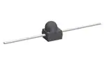
PACKAGE DIMENSIONS in millimeters: TEMD1000
16159
PACKAGE DIMENSIONS in millimeters: TEMD1020
3.8 ± 0.2
2.7 ± 0.2
0.75
0.15 ± 0.05
1.4
0.85
Ø 1.9 ± 0.2
0.3
0.4
C
Rev. 2.5, 04-Jun-2019
4.5 ± 0.1
0.5
2 ± 0.2
1.1
A
2.3 ± 0.1
1 ± 0.1
2.5 ± 0.2
16160
Document Number: 81564
4
For technical questions, contact: detectortechsupport@vishay.com
THIS DOCUMENT IS SUBJECT TO CHANGE WITHOUT NOTICE. THE PRODUCTS DESCRIBED HEREIN AND THIS DOCUMENT
ARE SUBJECT TO SPECIFIC DISCLAIMERS, SET FORTH AT www.vishay.com/doc?91000
�TEMD1000, TEMD1020, TEMD1030, TEMD1040
www.vishay.com
Vishay Semiconductors
PACKAGE DIMENSIONS in millimeters: TEMD1030
16228
PACKAGE DIMENSIONS in millimeters: TEMD1040
16760
Rev. 2.5, 04-Jun-2019
Document Number: 81564
5
For technical questions, contact: detectortechsupport@vishay.com
THIS DOCUMENT IS SUBJECT TO CHANGE WITHOUT NOTICE. THE PRODUCTS DESCRIBED HEREIN AND THIS DOCUMENT
ARE SUBJECT TO SPECIFIC DISCLAIMERS, SET FORTH AT www.vishay.com/doc?91000
�TEMD1000, TEMD1020, TEMD1030, TEMD1040
www.vishay.com
Vishay Semiconductors
REEL DIMENSIONS in millimeters
Unreel direction
X
2.
60.2
±0.5
16 ±0.2
5
178 ±1
.5
±0
0.
5
Tape position
coming out from reel
13
±
X
13.2
±1.5
Label posted here
Leader and trailer tape:
Empty leader (400 mm, min.)
Parts mounted
Drawing-No.: 9.800-5080.01-4
Direction of pulling out
Issue: 3; 11.06.08
Empty trailer (200 mm, min.)
18033
TAPING DIMENSIONS in millimeters: TEMD1000
3.05 ± 0.1
Top tape
Anode
Feed direction
12 ± 0.3
1.75 ± 0.1
2 ± 0.05
Ø 1.55 ± 0.05
5.5 ± 0.05
0.3
4 ± 0.1
4 ± 0.1
Push pin through hole
Quantity per reel: 1000 pcs or 5000 pcs
Rev. 2.5, 04-Jun-2019
18030
Document Number: 81564
6
For technical questions, contact: detectortechsupport@vishay.com
THIS DOCUMENT IS SUBJECT TO CHANGE WITHOUT NOTICE. THE PRODUCTS DESCRIBED HEREIN AND THIS DOCUMENT
ARE SUBJECT TO SPECIFIC DISCLAIMERS, SET FORTH AT www.vishay.com/doc?91000
�TEMD1000, TEMD1020, TEMD1030, TEMD1040
www.vishay.com
Vishay Semiconductors
TAPING DIMENSIONS in millimeters: TEMD1020
3.05 ± 0.1
4 ± 0.1
Feed direction
Top tape
12 ± 0.3
2 ± 0.05
1.75 ± 0.1
Ø 1.55 ± 0.05
5.5 ± 0.05
0.3
4 ± 0.1
Anode
Push pin through hole
Quantity per reel: 1000 pcs or 5000 pcs
18031
TAPING DIMENSIONS in millimeters: TEMD1030
3.05 ± 0.1
Feed direction
Top tape
4 ± 0.1
Anode
Push pin through hole
Rev. 2.5, 04-Jun-2019
12 ± 0.3
1.75 ± 0.1
2 ± 0.05
Ø 1.55 ± 0.05
5.5 ± 0.05
0.3
4 ± 0.1
18032
Quantity per reel: 1000 pcs or 5000 pcs
Document Number: 81564
7
For technical questions, contact: detectortechsupport@vishay.com
THIS DOCUMENT IS SUBJECT TO CHANGE WITHOUT NOTICE. THE PRODUCTS DESCRIBED HEREIN AND THIS DOCUMENT
ARE SUBJECT TO SPECIFIC DISCLAIMERS, SET FORTH AT www.vishay.com/doc?91000
�Legal Disclaimer Notice
www.vishay.com
Vishay
Disclaimer
ALL PRODUCT, PRODUCT SPECIFICATIONS AND DATA ARE SUBJECT TO CHANGE WITHOUT NOTICE TO IMPROVE
RELIABILITY, FUNCTION OR DESIGN OR OTHERWISE.
Vishay Intertechnology, Inc., its affiliates, agents, and employees, and all persons acting on its or their behalf (collectively,
“Vishay”), disclaim any and all liability for any errors, inaccuracies or incompleteness contained in any datasheet or in any other
disclosure relating to any product.
Vishay makes no warranty, representation or guarantee regarding the suitability of the products for any particular purpose or
the continuing production of any product. To the maximum extent permitted by applicable law, Vishay disclaims (i) any and all
liability arising out of the application or use of any product, (ii) any and all liability, including without limitation special,
consequential or incidental damages, and (iii) any and all implied warranties, including warranties of fitness for particular
purpose, non-infringement and merchantability.
Statements regarding the suitability of products for certain types of applications are based on Vishay's knowledge of typical
requirements that are often placed on Vishay products in generic applications. Such statements are not binding statements
about the suitability of products for a particular application. It is the customer's responsibility to validate that a particular product
with the properties described in the product specification is suitable for use in a particular application. Parameters provided in
datasheets and / or specifications may vary in different applications and performance may vary over time. All operating
parameters, including typical parameters, must be validated for each customer application by the customer's technical experts.
Product specifications do not expand or otherwise modify Vishay's terms and conditions of purchase, including but not limited
to the warranty expressed therein.
Hyperlinks included in this datasheet may direct users to third-party websites. These links are provided as a convenience and
for informational purposes only. Inclusion of these hyperlinks does not constitute an endorsement or an approval by Vishay of
any of the products, services or opinions of the corporation, organization or individual associated with the third-party website.
Vishay disclaims any and all liability and bears no responsibility for the accuracy, legality or content of the third-party website
or for that of subsequent links.
Except as expressly indicated in writing, Vishay products are not designed for use in medical, life-saving, or life-sustaining
applications or for any other application in which the failure of the Vishay product could result in personal injury or death.
Customers using or selling Vishay products not expressly indicated for use in such applications do so at their own risk. Please
contact authorized Vishay personnel to obtain written terms and conditions regarding products designed for such applications.
No license, express or implied, by estoppel or otherwise, to any intellectual property rights is granted by this document or by
any conduct of Vishay. Product names and markings noted herein may be trademarks of their respective owners.
© 2022 VISHAY INTERTECHNOLOGY, INC. ALL RIGHTS RESERVED
Revision: 01-Jan-2022
1
Document Number: 91000
�


 工商网监
湘ICP备2023018690号
工商网监
湘ICP备2023018690号
