TEMT6000X01
www.vishay.com
Vishay Semiconductors
Ambient Light Sensor
FEATURES
•
•
•
•
•
•
•
•
•
•
18527
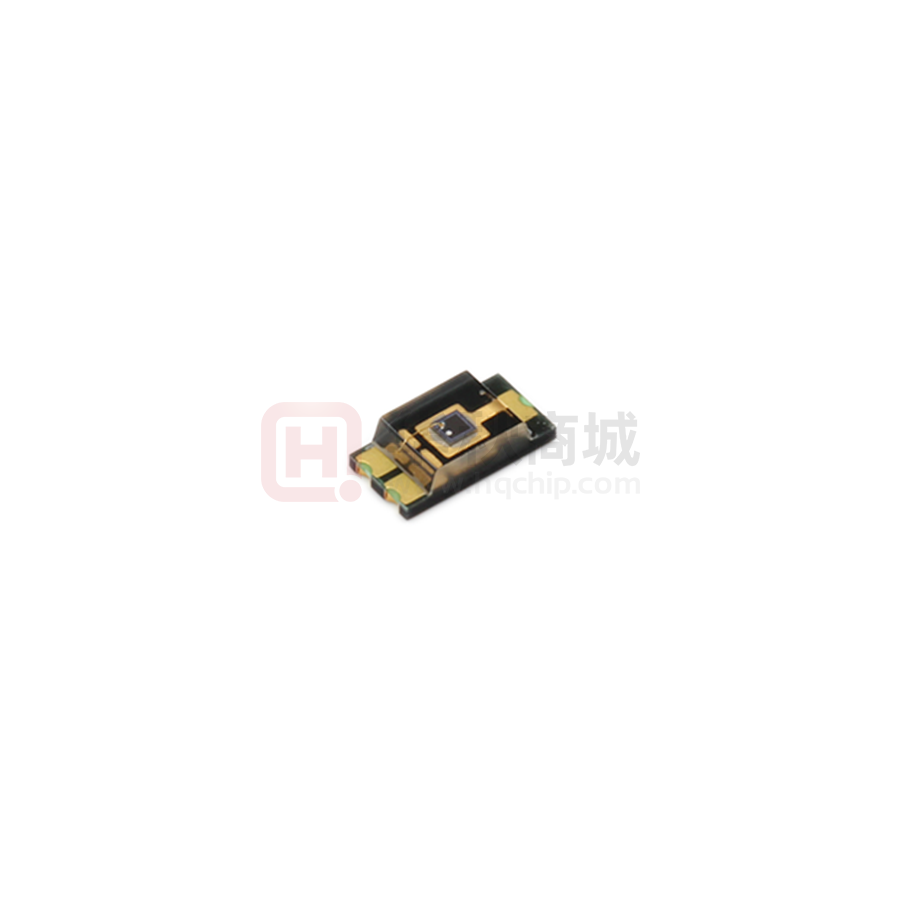
Package type: surface mount
Package form: 1206
Dimensions (L x W x H in mm): 4 x 2 x 1.05
AEC-Q101 qualified
High photo sensitivity
Adapted to human eye responsivity
Angle of half sensitivity: = ± 60°
Floor life: 168 h, MSL 3, acc. J-STD-020
Lead (Pb)-free reflow soldering
Compliant to RoHS Directive 2002/95/EC and in
accordance to WEEE 2002/96/EC
Note
** Please see document “Vishay Material Category Policy”:
www.vishay.com/doc?99902
DESCRIPTION
TEMT6000X01 ambient light sensor is a silicon NPN
epitaxial planar phototransistor in a miniature transparent
1206 package for surface mounting. It is sensitive to visible
light much like the human eye and has peak sensitivity at
570 nm.
APPLICATIONS
Ambient light sensor for control of display backlight dimming
in LCD displays and keypad backlighting of mobile devices
and in industrial on/off-lighting operation.
•
•
•
•
•
•
Automotive sensors
Mobile phones
Notebook computers
PDA’s
Cameras
Dashboards
PRODUCT SUMMARY
COMPONENT
IPCE (μA)
(deg)
0.5 (nm)
TEMT6000X01
50
± 60
440 to 800
Note
• Test condition see table “Basic Characteristics”
ORDERING INFORMATION
ORDERING CODE
PACKAGING
REMARKS
PACKAGE FORM
TEMT6000X01
Tape and reel
MOQ: 3000 pcs, 3000 pcs/reel
1206
Note
• MOQ: minimum order quantity
ABSOLUTE MAXIMUM RATINGS (Tamb = 25 °C, unless otherwise specified)
SYMBOL
VALUE
UNIT
Collector emitter voltage
VCEO
6
V
Emitter collector voltage
VECO
1.5
V
Collector current
IC
20
mA
Power dissipation
PV
100
mW
PARAMETER
Rev. 1.9, 23-Aug-11
TEST CONDITION
Document Number: 81579
1
For technical questions, contact: detectortechsupport@vishay.com
THIS DOCUMENT IS SUBJECT TO CHANGE WITHOUT NOTICE. THE PRODUCTS DESCRIBED HEREIN AND THIS DOCUMENT
ARE SUBJECT TO SPECIFIC DISCLAIMERS, SET FORTH AT www.vishay.com/doc?91000
�TEMT6000X01
www.vishay.com
Vishay Semiconductors
ABSOLUTE MAXIMUM RATINGS (Tamb = 25 °C, unless otherwise specified)
TEST CONDITION
SYMBOL
VALUE
UNIT
Tj
100
°C
Operating temperature range
Tamb
- 40 to + 100
°C
Storage temperature range
Tstg
- 40 to + 100
°C
Acc. reflow solder profile fig. 8
Tsd
260
°C
Soldered on PCB with pad dimensions: 4 mm x 4 mm
RthJA
450
K/W
PARAMETER
Junction temperature
Soldering temperature
Thermal resistance junction/ambient
PV - Power Dissipation (mW)
125
100
75
RthJA = 450 K/W
50
25
0
0
94 8308
20
40
60
100
80
Tamb - Ambient Temperature (°C)
Fig. 1 - Power Dissipation Limit vs. Ambient Temperature
BASIC CHARACTERISTICS (Tamb = 25 °C, unless otherwise specified)
TYP.
MAX.
UNIT
ICEO
3
50
nA
VCE = 0 V, f = 1 MHz, E = 0
CCEO
16
EV = 20 lx, CIE illuminant A,
VCE = 5 V
IPCE
EV = 100 lx, CIE illuminant A,
VCE = 5 V
IPCE
50
CIE illuminant A
TKIPCE
1.18
%/K
LED, white
TKIPCE
0.9
%/K
Angle of half sensitivity
± 60
deg
Wavelength of peak sensitivity
p
570
nm
Range of spectral bandwidth
0.5
440 to 800
nm
VCEsat
0.1
V
PARAMETER
Collector emitter breakdown voltage
Collector dark current
Collector emitter capacitance
Collector light current
Temperature coefficient of IPCE
Collector emitter saturation voltage
Rev. 1.9, 23-Aug-11
TEST CONDITION
SYMBOL
MIN.
IC = 0.1 mA
VCEO
6
VCE = 5 V, E = 0
EV = 20 lx, CIE illuminant A,
IPCE = 1.2 μA
3.5
V
10
pF
16
μA
μA
Document Number: 81579
2
For technical questions, contact: detectortechsupport@vishay.com
THIS DOCUMENT IS SUBJECT TO CHANGE WITHOUT NOTICE. THE PRODUCTS DESCRIBED HEREIN AND THIS DOCUMENT
ARE SUBJECT TO SPECIFIC DISCLAIMERS, SET FORTH AT www.vishay.com/doc?91000
�TEMT6000X01
www.vishay.com
Vishay Semiconductors
VCE = 5 V
10 -7
10 -8
10 -9
10 -10
10 -11
10 -12
10 -13
- 40
19758
- 20 0
20
40
60
80
Tamb - Ambient Temperature (°C)
100
15
10
5
0
0.1
1.0
10.0
VCE - Collector Emitter Voltage (V)
1.0
S(λ)rel - Relative Spectral Sensitivity
IPCE rel - Relative Photo Current
20
Fig. 4 - Collector Emitter Capacitance vs. Collector Emitter Voltage
2.2
2.0
1.8
1.6
1.4
1.2
1.0
0.8
0.6
0.4
0.2
19759
f = 1 MHz
19762
Fig. 1 - Collector Dark Current vs. Ambient Temperature
0
25
VCE = 5 V, white LED
- 40 - 20 0
20 40 60 80
Tamb - Ambient Temperature (°C)
0.9
0.8
0.7
0.6
0.5
0.4
0.3
0.2
0.1
100
20019
Fig. 2 - Relative Photo Current vs. Ambient Temperature
0.0
300 400 500 600 700 800 900 1000 1100
λ - Wavelength (nm)
Fig. 5 - Relative Spectral Sensitivity vs. Wavelength
0°
10°
20°
30°
Srel - Relative Sensitivity
IPCE - Photo Current (µA)
1000
100
10
40°
1.0
0.9
50°
0.8
60°
70°
0.7
ϕ - Angular Displacement
ICEO - Collector Dark Current (A)
10 -6
CCE0 - Collector Emitter Capacitance (pF)
BASIC CHARACTERISTICS (Tamb = 25 °C, unless otherwise specified)
80°
1
10
19760
100
E v - Illuminance (Ix)
Fig. 3 - Photo Current vs. Illuminance
Rev. 1.9, 23-Aug-11
0.6
1000
0.4
0.2
0
94 8318
Fig. 6 - Relative Radiant Sensitivity vs. Angular Displacement
Document Number: 81579
3
For technical questions, contact: detectortechsupport@vishay.com
THIS DOCUMENT IS SUBJECT TO CHANGE WITHOUT NOTICE. THE PRODUCTS DESCRIBED HEREIN AND THIS DOCUMENT
ARE SUBJECT TO SPECIFIC DISCLAIMERS, SET FORTH AT www.vishay.com/doc?91000
�TEMT6000X01
www.vishay.com
Vishay Semiconductors
REFLOW SOLDER PROFILE
DRYPACK
300
255 °C
240 °C
217 °C
250
Temperature (°C)
max. 260 °C
245 °C
Devices are packed in moisture barrier bags (MBB) to
prevent the products from moisture absorption during
transportation and storage. Each bag contains a desiccant.
FLOOR LIFE
200
max. 30 s
150
max. 100 s
max. 120 s
100
max. ramp up 3 °C/s max. ramp down 6 °C/s
50
Time between soldering and removing from MBB must not
exceed the time indicated in J-STD-020:
Moisture sensitivity: level 3
Floor life: 168 h
Conditions: Tamb < 30 °C, RH < 60 %
DRYING
0
0
19841
50
100
150
200
250
300
Time (s)
Fig. 7 - Lead (Pb)-free Reflow Solder Profile acc. J-STD-020D
In case of moisture absorption devices should be baked
before soldering. Conditions see J-STD-020 or label.
Devices taped on reel dry using recommended conditions:
192 h at 40 °C (+ 5 °C), RH < 5 %
or
96 h at 60 °C (+ 5 °C), RH < 5 %.
PACKAGE DIMENSIONS in millimeters
18464
Rev. 1.9, 23-Aug-11
Document Number: 81579
4
For technical questions, contact: detectortechsupport@vishay.com
THIS DOCUMENT IS SUBJECT TO CHANGE WITHOUT NOTICE. THE PRODUCTS DESCRIBED HEREIN AND THIS DOCUMENT
ARE SUBJECT TO SPECIFIC DISCLAIMERS, SET FORTH AT www.vishay.com/doc?91000
�TEMT6000X01
www.vishay.com
Vishay Semiconductors
BLISTER TAPE DIMENSIONS in millimeters
20876
REEL DIMENSIONS in millimeters
Volume: 3000 pcs/reel
20874
Rev. 1.9, 23-Aug-11
Document Number: 81579
5
For technical questions, contact: detectortechsupport@vishay.com
THIS DOCUMENT IS SUBJECT TO CHANGE WITHOUT NOTICE. THE PRODUCTS DESCRIBED HEREIN AND THIS DOCUMENT
ARE SUBJECT TO SPECIFIC DISCLAIMERS, SET FORTH AT www.vishay.com/doc?91000
�Legal Disclaimer Notice
www.vishay.com
Vishay
Disclaimer
ALL PRODUCT, PRODUCT SPECIFICATIONS AND DATA ARE SUBJECT TO CHANGE WITHOUT NOTICE TO IMPROVE
RELIABILITY, FUNCTION OR DESIGN OR OTHERWISE.
Vishay Intertechnology, Inc., its affiliates, agents, and employees, and all persons acting on its or their behalf (collectively,
“Vishay”), disclaim any and all liability for any errors, inaccuracies or incompleteness contained in any datasheet or in any other
disclosure relating to any product.
Vishay makes no warranty, representation or guarantee regarding the suitability of the products for any particular purpose or
the continuing production of any product. To the maximum extent permitted by applicable law, Vishay disclaims (i) any and all
liability arising out of the application or use of any product, (ii) any and all liability, including without limitation special,
consequential or incidental damages, and (iii) any and all implied warranties, including warranties of fitness for particular
purpose, non-infringement and merchantability.
Statements regarding the suitability of products for certain types of applications are based on Vishay’s knowledge of
typical requirements that are often placed on Vishay products in generic applications. Such statements are not binding
statements about the suitability of products for a particular application. It is the customer’s responsibility to validate that a
particular product with the properties described in the product specification is suitable for use in a particular application.
Parameters provided in datasheets and / or specifications may vary in different applications and performance may vary over
time. All operating parameters, including typical parameters, must be validated for each customer application by the customer’s
technical experts. Product specifications do not expand or otherwise modify Vishay’s terms and conditions of purchase,
including but not limited to the warranty expressed therein.
Except as expressly indicated in writing, Vishay products are not designed for use in medical, life-saving, or life-sustaining
applications or for any other application in which the failure of the Vishay product could result in personal injury or death.
Customers using or selling Vishay products not expressly indicated for use in such applications do so at their own risk.
Please contact authorized Vishay personnel to obtain written terms and conditions regarding products designed for
such applications.
No license, express or implied, by estoppel or otherwise, to any intellectual property rights is granted by this document
or by any conduct of Vishay. Product names and markings noted herein may be trademarks of their respective owners.
© 2021 VISHAY INTERTECHNOLOGY, INC. ALL RIGHTS RESERVED
Revision: 01-Jan-2021
1
Document Number: 91000
�


 工商网监
湘ICP备2023018690号
工商网监
湘ICP备2023018690号

