TP0610KL/BS250KL
Vishay Siliconix
P-Channel 60-V (D-S) MOSFET
FEATURES
PRODUCT SUMMARY
V(BR)DSS(min) (V)
rDS(on) (�)
VGS(th) (V)
6 @ VGS = −10 V
−60
60
10 @ VGS = −4.5 V
ID (A)
1
2
D
3
“S” TP
0610KL
xxyy
Device Marking
Front View
G
2
S
3
“S” = Siliconix Logo
xxyy = Date Code
Ordering Information: TP0610KL-TR1
D
1
D
Top View
D Drivers: Relays, Solenoids, Lamps, Hammers,
Displays, Memories, Transistors, etc.
D Battery Operated Systems
D Power Supply, Converter Circuits
D Motor Control
−0.21
Device Marking
Front View
G
APPLICATIONS
−0.27
−1
1 to −3.0
30
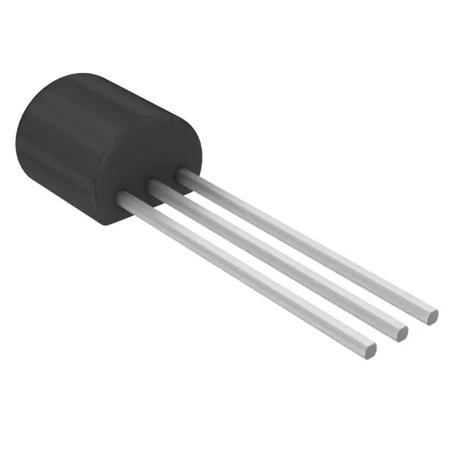
TO-92-18RM
(TO-18 Lead Form)
TO-226AA
(TO-92)
S
D TrenchFETr Power MOSFET
D ESD Protected: 2000 V
“S” BS
250KL
xxyy
Top View
100 �
G
“S” = Siliconix Logo
xxyy = Date Code
S
Ordering Information: BS250KL-TR1
ABSOLUTE MAXIMUM RATINGS (TA = 25_C UNLESS OTHERWISE NOTED)
Parameter
Symbol
Limit
Drain-Source Voltage
VDS
−60
Gate-Source Voltage
VGS
"20
Continuous Drain Current
Pulse Drain
TA = 25_C
TA = 70_C
Currenta
Power Dissipation
Maximum Junction-to-Ambient
Operating Junction and Storage Temperature Range
ID
IDM
TA = 25_C
TA = 70_C
PD
Unit
V
−0.27
−0.22
A
−1.0
0.8
0.51
W
RthJA
156
_C/W
TJ, Tstg
−55 to 150
_C
Notes
a. Pulse width limited by maximum junction temperature.
Document Number: 72712
S-40244—Rev. A, 16-Feb-04
www.vishay.com
1
�TP0610KL/BS250KL
Vishay Siliconix
SPECIFICATIONS (TA = 25_C UNLESS OTHERWISE NOTED)
Parameter
Symbol
Test Condition
Min
V(BR)DSS
VGS = 0 V, ID = −10 µA
−60
VGS(th)
VDS = VGS, ID = −250 µA
−1
Typ
Max
−2.1
−3.0
Unit
Static
Drain-Source Breakdown Voltage
Gate-Threshold Voltage
Gate Body Leakage
Gate-Body
IGSS
Zero Gate Voltage Drain Current
IDSS
On State Drain Currenta
On-State
ID(on)
D( )
Drain-Source On-Resistancea
Forward Transconductancea
Diode Forward
Voltagea
VDS = 0 V, VGS = "20 V
"10
VDS = 0 V, VGS = "10 V
"200
VDS = 0 V, VGS = "10 V, TJ = 85_C
"500
VDS = 0 V, VGS = "5 V
"100
VDS = −60 V, VGS = 0 V
−1
VDS = −60 V, VGS = 0 V, TJ = 55_C
−10
VDS = −10 V, VGS = −4.5 V
−50
VDS = −10 V, VGS = −10 V
−600
�A
nA
�A
mA
VGS = −4.5 V, ID = −25 mA
5.5
10
VGS = −10 V, ID = −500 mA
3.1
6
VGS = −10 V, ID = −500 mA, TJ = 125_C
4.7
9
gfs
VDS = −10 V, ID = −100 mA
180
VSD
IS = −200 mA, VGS = 0 V
−0.9
−1.4
1.7
3
VDS = −30 V, VGS = −15 V, ID ^ −500 mA
0.26
rDS(on)
V
�
mS
V
Dynamicb
Total Gate Charge
Qg
Gate-Source Charge
Qgs
Gate-Drain Charge
Qgd
0.46
Rg
285
td(on)
2.4
5
15.5
25
21
35
12.5
20
Gate Resistance
Turn On Time
Turn-On
VDD = −25 V, RL = 150 �
ID ^ −150 mA,
mA VGEN = −10 V
Rg = 10 �
tr
td(off)
Turn Off Time
Turn-Off
tf
nC
�
ns
Notes
a. Pulse test: PW v300 ms duty cycle v2%.
b. Guaranteed by design, not subject to production testing.
TYPICAL CHARACTERISTICS (25_C UNLESS NOTED)
For the following graphs, p-channel negative polarities for all voltage and current values are represented as positive values.
Output Characteristics
1.0
Transfer Characteristics
1200
VGS = 10 V
8V
7V
0.6
I D − Drain Current (mA)
0.8
I D − Drain Current (A)
TJ = −55_C
6V
0.4
5V
0.2
900
25_C
125_C
600
300
4V
0.0
0
0
1
2
3
4
VDS − Drain-to-Source Voltage (V)
www.vishay.com
2
5
0
2
4
6
8
10
VGS − Gate-to-Source Voltage (V)
Document Number: 72712
S-40244—Rev. A, 16-Feb-04
�TP0610KL/BS250KL
Vishay Siliconix
TYPICAL CHARACTERISTICS (25_C UNLESS NOTED)
For the following graphs, p-channel negative polarities for all voltage and current values are represented as positive values.
On-Resistance vs. Drain Current
20
Capacitance
40
VGS = 4.5 V
16
32
C − Capacitance (pF)
r DS(on) − On-Resistance ( � )
VGS = 0 V
12
VGS = 5 V
8
VGS = 10 V
4
Ciss
24
16
Coss
8
Crss
0
0
0
200
400
600
800
0
1000
5
ID − Drain Current (mA)
25
1.5
VDS = 30 V
VGS = 10 V @ 500 mA
rDS(on) − On-Resiistance
(Normalized)
V GS − Gate-to-Source Voltage (V)
ID = 500 mA
VDS = 48 V
9
6
3
0
0.0
20
On-Resistance vs. Junction Temperature
1.8
12
15
VDS − Drain-to-Source Voltage (V)
Gate Charge
15
10
1.2
VGS = 4.5 V @ 25 mA
0.9
0.6
0.3
0.3
0.6
0.9
1.2
1.5
0.0
−50
1.8
Qg − Total Gate Charge (nC)
−25
0
25
50
75
100
125
150
TJ − Junction Temperature (_C)
Source-Drain Diode Forward Voltage
On-Resistance vs. Gate-Source Voltage
10
1000
r DS(on) − On-Resistance ( � )
I S − Source Current (A)
VGS = 0 V
100
TJ = 125_C
10
TJ = 25_C
TJ = −55_C
ID = 500 mA
6
4
ID = 200 mA
2
0
1
0.00
8
0.3
0.6
0.9
1.2
VSD − Source-to-Drain Voltage (V)
Document Number: 72712
S-40244—Rev. A, 16-Feb-04
1.5
0
2
4
6
8
10
VGS − Gate-to-Source Voltage (V)
www.vishay.com
3
�TP0610KL/BS250KL
Vishay Siliconix
TYPICAL CHARACTERISTICS (25_C UNLESS NOTED)
For the following graphs, p-channel negative polarities for all voltage and current values are represented as positive values.
Threshold Voltage Variance Over Temperature
Single Pulse Power, Junction-to-Ambient
0.5
20
ID = 250 �A
16
0.3
0.2
Power (W)
V GS(th) Variance (V)
0.4
0.1
−0.0
−0.1
12
8
4
−0.2
−0.3
−50
0
−25
0
25
50
75
100
125
150
0.01
0.1
1
10
100
600
Time (sec)
TJ − Junction Temperature (_C)
10
Safe Operating Area
IDM
Limited
rDS(on) Limited
I D − Drain Current (A)
1
1 ms
10 ms
100 ms
0.1
1s
ID(on)
Limited
0.01
10 s
dc
TA = 25_C
Single Pulse
BVDSS Limited
0.001
0.1
1
10
100
VDS − Drain-to-Source Voltage (V)
Normalized Thermal Transient Impedance, Junction-to-Ambient
Normalized Effective Transient
Thermal Impedance
2
1
Duty Cycle = 0.5
0.2
Notes:
0.1
PDM
0.1
0.05
t1
t2
1. Duty Cycle, D =
0.02
t1
t2
2. Per Unit Base = RthJA = 156_C/W
3. TJM − TA = PDMZthJA(t)
Single Pulse
4. Surface Mounted
0.01
10−4
www.vishay.com
4
10−3
10−2
10−1
1
Square Wave Pulse Duration (sec)
10
100
600
Document Number: 72712
S-40244—Rev. A, 16-Feb-04
�Legal Disclaimer Notice
Vishay
Disclaimer
All product specifications and data are subject to change without notice.
Vishay Intertechnology, Inc., its affiliates, agents, and employees, and all persons acting on its or their behalf
(collectively, “Vishay”), disclaim any and all liability for any errors, inaccuracies or incompleteness contained herein
or in any other disclosure relating to any product.
Vishay disclaims any and all liability arising out of the use or application of any product described herein or of any
information provided herein to the maximum extent permitted by law. The product specifications do not expand or
otherwise modify Vishay’s terms and conditions of purchase, including but not limited to the warranty expressed
therein, which apply to these products.
No license, express or implied, by estoppel or otherwise, to any intellectual property rights is granted by this
document or by any conduct of Vishay.
The products shown herein are not designed for use in medical, life-saving, or life-sustaining applications unless
otherwise expressly indicated. Customers using or selling Vishay products not expressly indicated for use in such
applications do so entirely at their own risk and agree to fully indemnify Vishay for any damages arising or resulting
from such use or sale. Please contact authorized Vishay personnel to obtain written terms and conditions regarding
products designed for such applications.
Product names and markings noted herein may be trademarks of their respective owners.
Document Number: 91000
Revision: 18-Jul-08
www.vishay.com
1
�Legal Disclaimer Notice
www.vishay.com
Vishay
Disclaimer
ALL PRODUCT, PRODUCT SPECIFICATIONS AND DATA ARE SUBJECT TO CHANGE WITHOUT NOTICE TO IMPROVE
RELIABILITY, FUNCTION OR DESIGN OR OTHERWISE.
Vishay Intertechnology, Inc., its affiliates, agents, and employees, and all persons acting on its or their behalf (collectively,
“Vishay”), disclaim any and all liability for any errors, inaccuracies or incompleteness contained in any datasheet or in any other
disclosure relating to any product.
Vishay makes no warranty, representation or guarantee regarding the suitability of the products for any particular purpose or
the continuing production of any product. To the maximum extent permitted by applicable law, Vishay disclaims (i) any and all
liability arising out of the application or use of any product, (ii) any and all liability, including without limitation special,
consequential or incidental damages, and (iii) any and all implied warranties, including warranties of fitness for particular
purpose, non-infringement and merchantability.
Statements regarding the suitability of products for certain types of applications are based on Vishay's knowledge of typical
requirements that are often placed on Vishay products in generic applications. Such statements are not binding statements
about the suitability of products for a particular application. It is the customer's responsibility to validate that a particular product
with the properties described in the product specification is suitable for use in a particular application. Parameters provided in
datasheets and / or specifications may vary in different applications and performance may vary over time. All operating
parameters, including typical parameters, must be validated for each customer application by the customer's technical experts.
Product specifications do not expand or otherwise modify Vishay's terms and conditions of purchase, including but not limited
to the warranty expressed therein.
Hyperlinks included in this datasheet may direct users to third-party websites. These links are provided as a convenience and
for informational purposes only. Inclusion of these hyperlinks does not constitute an endorsement or an approval by Vishay of
any of the products, services or opinions of the corporation, organization or individual associated with the third-party website.
Vishay disclaims any and all liability and bears no responsibility for the accuracy, legality or content of the third-party website
or for that of subsequent links.
Except as expressly indicated in writing, Vishay products are not designed for use in medical, life-saving, or life-sustaining
applications or for any other application in which the failure of the Vishay product could result in personal injury or death.
Customers using or selling Vishay products not expressly indicated for use in such applications do so at their own risk. Please
contact authorized Vishay personnel to obtain written terms and conditions regarding products designed for such applications.
No license, express or implied, by estoppel or otherwise, to any intellectual property rights is granted by this document or by
any conduct of Vishay. Product names and markings noted herein may be trademarks of their respective owners.
© 2022 VISHAY INTERTECHNOLOGY, INC. ALL RIGHTS RESERVED
Revision: 01-Jan-2022
1
Document Number: 91000
�