End of Life May-2023 - Alternative Device: TSMP91100
TSMP1138
www.vishay.com
Vishay Semiconductors
IR Sensor Module for Remote Control Systems
FEATURES
• Photo detector and preamplifier in one package
• AC coupled response from 30 kHz to 60 kHz, all
data formats
• If the IR signal strength is more then 500 mW/m2
(distance less than 0.5 m with a typical IR remote
control), the frequency range is limited to 55 kHz
• Improved shielding
disturbance
against
electrical
field
• AGC to suppress ambient noise
948691
• High sensitivity, long receiving range
LINKS TO ADDITIONAL RESOURCES
• Supply voltage: 2.5 V to 5.5 V
3D 3D
Product Page
3D Models
• Carrier out signal for IR repeater applications
Marking
Packages
• Material categorization: for definitions of compliance
please see www.vishay.com/doc?99912
Holders
Bends and Cuts
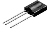
MECHANICAL DATA
Pinning:
DESCRIPTION
1 = GND, 2 = carrier OUT, 3 = VS
The TSMP1138 is a miniaturized sensor for receiving the
modulated signal of infrared remote control systems. A PIN
diode and preamplifier are assembled on a lead frame, the
epoxy package is designed as an IR filter. The modulated
output signal, carrier out, can be used for repeater
applications and code learning applications.
ORDERING CODE
TSMP1138 - 1000 pieces in tubes
BLOCK DIAGRAM
This component has not been qualified according to
automotive specifications.
16833_11
3
VS
33 kΩ
2
Input
AGC
Band
pass
OUT
Comparator
1
PIN
Control circuit
GND
APPLICATION CIRCUIT
680 Ω
TSMPxxxxx
1 μF
Supply
voltage
+3 V or +5 V
TSAL6400
100 Ω
47 μF
33 kΩ
3Ω
In case of a supply voltage of
3 V, use one IR emitter only
GND
0V
Recommended circuit for best sensitivity in repeater applications.
It limits the output voltage swing VO to about 0.7 V in order to avoid internal coupling.
Rev. 1.8, 11-Oct-2022
1
Document Number: 82484
THIS DOCUMENT IS SUBJECT TO CHANGE WITHOUT NOTICE. THE PRODUCTS DESCRIBED HEREIN AND THIS DOCUMENT
ARE SUBJECT TO SPECIFIC DISCLAIMERS, SET FORTH AT www.vishay.com/doc?91000
�End of Life May-2023 - Alternative Device: TSMP91100
TSMP1138
www.vishay.com
Vishay Semiconductors
PARTS TABLE
Carrier frequency
38 kHz
TSMP1138
Package
Cast
Pinning
1 = GND, 2 = carrier OUT, 3 = VS
Dimensions (mm)
10.0 W x 12.5 H x 5.8 D
Mounting
Leaded
Application
Repeater
ABSOLUTE MAXIMUM RATINGS
PARAMETER
SYMBOL
VALUE
Supply voltage (pin 3)
TEST CONDITION
VS
-0.3 to +6
V
Supply current (pin 3)
IS
5
mA
Output voltage (pin 2)
VO
-0.3 to 5.5
V
VS - VO
-0.3 to (VS + 0.3)
V
IO
5
mA
Voltage at output to supply
Output current (pin 2)
Junction temperature
Storage temperature range
Operating temperature range
Power consumption
Soldering temperature
UNIT
Tj
100
°C
Tstg
-25 to +85
°C
Tamb
-25 to +85
°C
Tamb ≤ 85 °C
Ptot
10
mW
t ≤ 10 s, 1 mm from case
Tsd
260
°C
Note
• Stresses beyond those listed under “Absolute Maximum Ratings” may cause permanent damage to the device. This is a stress rating only
and functional operation of the device at these or any other conditions beyond those indicated in the operational sections of this specification
is not implied. Exposure to absolute maximum rating conditions for extended periods may affect the device reliability
ELECTRICAL AND OPTICAL CHARACTERISTICS (Tamb = 25 °C, unless otherwise specified)
PARAMETER
TEST CONDITION
SYMBOL
MIN.
TYP.
MAX.
Ev = 0, VS = 5 V
ISD
0.55
0.7
0.9
mA
Ev = 40 klx, sunlight
ISH
-
0.8
-
mA
VS
2.5
-
5.5
V
Ev = 0, test signal see Fig. 1,
IR diode TSAL6200,
IF = 50 mA
d
-
10
-
m
IOSL = 0.5 mA, Ee = 0.7 mW/m2,
test signal see Fig. 1
VOSL
-
-
100
mV
Minimum irradiance
Less than 5 missing or 5 additional
sub carrier pulses related to one
burst
Ee min.
-
0.5
1
mW/m2
Maximum irradiance
Less than 5 missing or 5 additional
sub carrier pulses related to one
burst
Ee max.
30
-
-
W/m2
Angle of half transmission
distance
ϕ1/2
-
± 55
-
deg
Supply current (pin 3)
Supply voltage
Transmission distance
Output voltage low (pin 2)
Directivity
Rev. 1.8, 11-Oct-2022
2
UNIT
Document Number: 82484
THIS DOCUMENT IS SUBJECT TO CHANGE WITHOUT NOTICE. THE PRODUCTS DESCRIBED HEREIN AND THIS DOCUMENT
ARE SUBJECT TO SPECIFIC DISCLAIMERS, SET FORTH AT www.vishay.com/doc?91000
�End of Life May-2023 - Alternative Device: TSMP91100
TSMP1138
www.vishay.com
Vishay Semiconductors
TYPICAL CHARACTERISTICS (Tamb = 25 °C, unless otherwise specified)
-20
Optical Test Signal:
IR diode TSAL6200, IF = 0.25 A,
N = 15 carrier pulses per burst, f = 38 kHz,
burst repetition time: 3 ms
Ee
-10
0
10
0.2
0
0.2
20
-30
-40
t
tpi - burst length
VO
tpi ≥ 6 carrier cycles is recommended for optimum function
VOH
VOL
0.6
t
The number of carrier- out-pulses might not be exactly
same as the number of carrier cycles in tpi (input burst)
21648
94 8153
0.4
0.6
Fig. 4 - Horizontal Directivity ϕx
Fig. 1 - Output Function
-20
3.5
Ee min. - Detection Threshold (mW/m²)
0.4
drel - Relative Transmission Distance
-10
0
10
0.2
0
0.2
20
-30
3.0
2.5
-40
2.0
y
1.5
x
1.0
0.5
0
30
35
21772
40
45
50
55
60
0.6
f0 - Carrier Frequency (kHz)
94 8152
0.4
0.4
0.6
drel - Relative Transmission Distance
Fig. 5 - Vertical Directivity ϕy
Fig. 2 - Frequency Dependence of Sensitivity
Axis Title
10000
0.9
0.8
0.7
1000
0.6
1st line
2nd line
2nd line
S(λ)rel. - Relative Spectral Sensitivity
1.0
0.5
0.4
100
0.3
0.2
0.1
0
750
850
950
1050
10
1150
λ - Wavelength (nm)
23180
Fig. 3 - Relative Spectral Sensitivity vs. Wavelength
Rev. 1.8, 11-Oct-2022
3
Document Number: 82484
THIS DOCUMENT IS SUBJECT TO CHANGE WITHOUT NOTICE. THE PRODUCTS DESCRIBED HEREIN AND THIS DOCUMENT
ARE SUBJECT TO SPECIFIC DISCLAIMERS, SET FORTH AT www.vishay.com/doc?91000
�End of Life May-2023 - Alternative Device: TSMP91100
TSMP1138
www.vishay.com
Vishay Semiconductors
PACKAGE DIMENSIONS in millimeters
10
± 0.3
(9.2)
0.65
+ 0.10
- 0.15
0.8 max.
30.6
± 0.5
12.5
± 0.4
Center of sensitive area
0.5
Area not plane
0.4
+ 0.15
- 0.05
2.54 nom.
+ 0.10
- 0.05
1.4 ± 0.3
4 ± 0.3
3 x 2.54 = 7.62 nom.
5.8
± 0.3
R 2.75
technical drawings
according to DIN
specifications
Drawing-No.: 6.550-5095.01-4
Issue: xx; 20.05.09
96 12116-1
Rev. 1.8, 11-Oct-2022
4
Document Number: 82484
THIS DOCUMENT IS SUBJECT TO CHANGE WITHOUT NOTICE. THE PRODUCTS DESCRIBED HEREIN AND THIS DOCUMENT
ARE SUBJECT TO SPECIFIC DISCLAIMERS, SET FORTH AT www.vishay.com/doc?91000
�Legal Disclaimer Notice
www.vishay.com
Vishay
Disclaimer
ALL PRODUCT, PRODUCT SPECIFICATIONS AND DATA ARE SUBJECT TO CHANGE WITHOUT NOTICE TO IMPROVE
RELIABILITY, FUNCTION OR DESIGN OR OTHERWISE.
Vishay Intertechnology, Inc., its affiliates, agents, and employees, and all persons acting on its or their behalf (collectively,
“Vishay”), disclaim any and all liability for any errors, inaccuracies or incompleteness contained in any datasheet or in any other
disclosure relating to any product.
Vishay makes no warranty, representation or guarantee regarding the suitability of the products for any particular purpose or
the continuing production of any product. To the maximum extent permitted by applicable law, Vishay disclaims (i) any and all
liability arising out of the application or use of any product, (ii) any and all liability, including without limitation special,
consequential or incidental damages, and (iii) any and all implied warranties, including warranties of fitness for particular
purpose, non-infringement and merchantability.
Statements regarding the suitability of products for certain types of applications are based on Vishay's knowledge of typical
requirements that are often placed on Vishay products in generic applications. Such statements are not binding statements
about the suitability of products for a particular application. It is the customer's responsibility to validate that a particular product
with the properties described in the product specification is suitable for use in a particular application. Parameters provided in
datasheets and / or specifications may vary in different applications and performance may vary over time. All operating
parameters, including typical parameters, must be validated for each customer application by the customer's technical experts.
Product specifications do not expand or otherwise modify Vishay's terms and conditions of purchase, including but not limited
to the warranty expressed therein.
Hyperlinks included in this datasheet may direct users to third-party websites. These links are provided as a convenience and
for informational purposes only. Inclusion of these hyperlinks does not constitute an endorsement or an approval by Vishay of
any of the products, services or opinions of the corporation, organization or individual associated with the third-party website.
Vishay disclaims any and all liability and bears no responsibility for the accuracy, legality or content of the third-party website
or for that of subsequent links.
Except as expressly indicated in writing, Vishay products are not designed for use in medical, life-saving, or life-sustaining
applications or for any other application in which the failure of the Vishay product could result in personal injury or death.
Customers using or selling Vishay products not expressly indicated for use in such applications do so at their own risk. Please
contact authorized Vishay personnel to obtain written terms and conditions regarding products designed for such applications.
No license, express or implied, by estoppel or otherwise, to any intellectual property rights is granted by this document or by
any conduct of Vishay. Product names and markings noted herein may be trademarks of their respective owners.
© 2022 VISHAY INTERTECHNOLOGY, INC. ALL RIGHTS RESERVED
Revision: 01-Jan-2022
1
Document Number: 91000
�