TSTS7100
Vishay Semiconductors
Infrared Emitting Diode, RoHS Compliant, 950 nm, GaAs
FEATURES
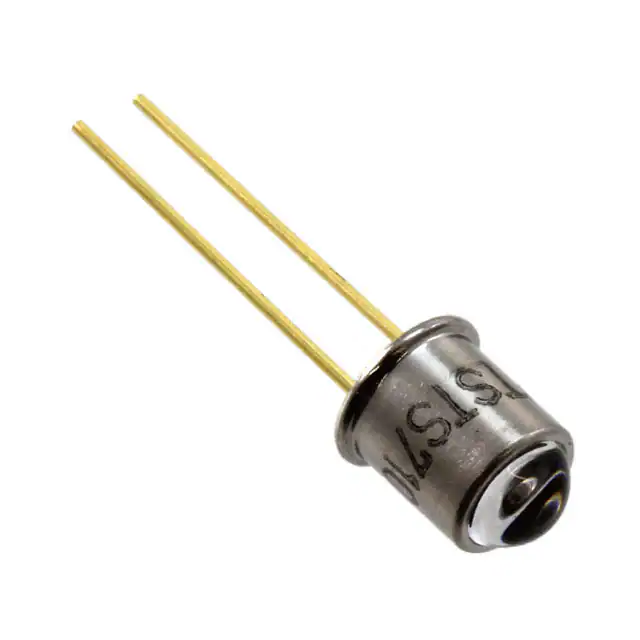
• Package type: leaded
• Package form: TO-18
• Dimensions (in mm): ∅ 4.7
• Peak wavelength: λp = 950 nm
• High reliability
• High radiant power
• High radiant intensity
• Angle of half intensity: ϕ = ± 5°
• Low forward voltage
94 8483
• Suitable for high pulse current operation
• Good spectral matching with Si photodetectors
DESCRIPTION
• Lead (Pb)-free component in accordance
RoHS 2002/95/EC and WEEE 2002/96/EC
TSTS7100 is an infrared, 950 nm emitting diode in GaAs
technology in a hermetically sealed TO-18 package with
lens.
APPLICATIONS
with
• Radiation source in near infrared range
PRODUCT SUMMARY
COMPONENT
Ie (mW/sr)
ϕ (deg)
λP (nm)
tr (ns)
> 10
±5
950
800
TSTS7100
Note
Test conditions see table “Basic Characteristics”
ORDERING INFORMATION
ORDERING CODE
PACKAGING
REMARKS
PACKAGE FORM
Bulk
MOQ: 1000 pcs, 1000 pcs/bulk
TO-18
TSTS7100
Note
MOQ: minimum order quantity
ABSOLUTE MAXIMUM RATINGS
PARAMETER
TEST CONDITION
SYMBOL
VALUE
VR
5
V
Tcase ≤ 25 °C
IF
250
mA
Peak forward current
tp/T = 0.5, tp ≤ 100 µs, Tcase ≤ 25 °C
IFM
500
mA
Surge forward current
tp ≤ 100 µs
IFSM
2.5
A
PV
170
mW
PV
500
mW
Tj
100
°C
Tstg
- 55 to + 100
°C
Reverse voltage
Forward current
Power dissipation
Tcase ≤ 25 °C
Junction temperature
Storage temperature range
UNIT
Thermal resistance junction/ambient
leads not soldered
RthJA
450
K/W
Thermal resistance junction/case
leads not soldered
RthJC
150
K/W
Note
Tamb = 25 °C, unless otherwise specified
www.vishay.com
260
For technical questions, contact: emittertechsupport@vishay.com
Document Number: 81047
Rev. 1.8, 04-Sep-08
�TSTS7100
Infrared Emitting Diode, RoHS Compliant, Vishay Semiconductors
950 nm, GaAs
300
R thJC
500
IF - Forward Current (mA)
PV - Power Dissipation (mW)
600
400
300
200
R thJA
250
200
RthJC
150
RthJA
100
50
100
0
0
0
25
50
75
100
125
0
Tamb - Ambient Temperature (°C)
12790
20
Fig. 1 - Power Dissipation Limit vs. Ambient Temperature
40
60
100
80
Tamb - Ambient Temperature (°C)
94 8018
Fig. 2 - Forward Current Limit vs. Ambient Temperature
BASIC CHARACTERISTICS
PARAMETER
TEST CONDITION
SYMBOL
TYP.
MAX.
IF = 100 mA, tp ≤ 20 ms
VF
1.3
1.7
IF = 100 mA
TKVF
- 1.3
mV/K
IR = 100 µA
V(BR)
VR = 0 V, f = 1 MHz, E = 0
Cj
30
pF
Forward voltage
Temperature coefficient of VF
Breakdown voltage
Junction capacitance
MIN.
UNIT
V
5
V
Radiant intensity
IF = 100 mA, tp = 20 ms
Ie
Radiant power
IF = 100 mA, tp ≤ 20 ms
φe
7
mW
IF = 100 mA
TKφe
- 0.8
%/K
ϕ
±5
deg
Peak wavelength
IF = 100 mA
λp
950
nm
Spectral bandwidth
IF = 100 mA
Δλ
50
nm
IF = 100 mA
tr
800
ns
IF = 1.5 A, tp/T = 0.01, tp ≤ 10 µs
tr
400
ns
d
1.5
mm
Temperature coefficient of φe
Angle of half intensity
Rise time
Virtual source diameter
10
50
mW/sr
Note
Tamb = 25 °C, unless otherwise specified
BASIC CHARACTERISTICS
Tamb = 25 °C, unless otherwise specified
10 4
I F - Forward Current (mA)
IF - Forward Current (A)
10 1
I FSM = 2.5 A (single pause)
t p /T= 0.01
10 0
0.05
0.1
0.2
10 3
10 2
10 1
10 0
0.5
10 -1
10 -2
94 8003
10 -1
10 -1
10 0
10 1
t p - Pulse Duration (ms)
10 2
Fig. 3 - Pulse Forward Current vs. Pulse Duration
Document Number: 81047
Rev. 1.8, 04-Sep-08
94 7996
0
1
2
3
4
V F - Forward Voltage (V)
Fig. 4 - Forward Current vs. Forward Voltage
For technical questions, contact: emittertechsupport@vishay.com
www.vishay.com
261
�TSTS7100
Vishay Semiconductors Infrared Emitting Diode, RoHS Compliant,
950 nm, GaAs
1.6
1.1
1.2
IF = 10 mA
Ie rel; Φe rel
VF rel - Relative Forward Voltage (V)
1.2
1.0
0.9
IF = 20 mA
0.8
0.4
0.8
0.7
0
20
40
60
80
Tamb - Ambient Temperature (°C)
94 7990
0
- 10 0 10
100
Fig. 5 - Relative Forward Voltage vs. Ambient Temperature
1.25
Φe rel - Relative Radiant Power
I e - Radiant Intensity (mW/sr)
100
10
1
t p /T = 0.01 , t p = 20 µs
1.0
0.75
0.5
0.25
IF = 100 mA
0
900
0.1
10 0
10 1
10 2
10 3
I F - Forward Current (mA)
10 4
Fig. 9 - Relative Radiant Power vs. Wavelength
0°
I e rel - Relative Radiant Intensity
1000
100
10
1
1000
950
λ - Wavelength (nm)
94 7994
Fig. 6 - Radiant Intensity vs. Forward Current
Φe - Radiant Power (mW)
140
100
Fig. 8 - Rel. Radiant Intensity/Power vs. Ambient Temperature
1000
94 8001
50
T amb - Ambient Temperature (°C)
94 7993
10°
20°
30°
40°
1.0
0.9
50°
0.8
60°
70°
0.7
80°
0.1
10 0
94 7977
10 1
10 2
10 3
I F - Forward Current (mA)
Fig. 7 - Radiant Power vs. Forward Current
www.vishay.com
262
0.6
10 4
0.4
0.2
0
0.2
0.4
0.6
94 8019
Fig. 10 - Relative Radiant Intensity vs. Angular Displacement
For technical questions, contact: emittertechsupport@vishay.com
Document Number: 81047
Rev. 1.8, 04-Sep-08
�TSTS7100
Infrared Emitting Diode, RoHS Compliant, Vishay Semiconductors
950 nm, GaAs
PACKAGE DIMENSIONS in millimeters
C
± 0.15
A
+ 0.05
- 0.10
6.5
± 0.25
4.7
5.5
2.54 nom.
13.2
± 0.7
(2.5)
Chip position
0.45
+ 0.02
- 0.05
3.9
Lens
± 0.05
technical drawings
according to DIN
specifications
Drawing-No.: 6.503-5002.02-4
Issue: 1; 24.08.98
14486
Document Number: 81047
Rev. 1.8, 04-Sep-08
For technical questions, contact: emittertechsupport@vishay.com
www.vishay.com
263
�Legal Disclaimer Notice
www.vishay.com
Vishay
Disclaimer
ALL PRODUCT, PRODUCT SPECIFICATIONS AND DATA ARE SUBJECT TO CHANGE WITHOUT NOTICE TO IMPROVE
RELIABILITY, FUNCTION OR DESIGN OR OTHERWISE.
Vishay Intertechnology, Inc., its affiliates, agents, and employees, and all persons acting on its or their behalf (collectively,
“Vishay”), disclaim any and all liability for any errors, inaccuracies or incompleteness contained in any datasheet or in any other
disclosure relating to any product.
Vishay makes no warranty, representation or guarantee regarding the suitability of the products for any particular purpose or
the continuing production of any product. To the maximum extent permitted by applicable law, Vishay disclaims (i) any and all
liability arising out of the application or use of any product, (ii) any and all liability, including without limitation special,
consequential or incidental damages, and (iii) any and all implied warranties, including warranties of fitness for particular
purpose, non-infringement and merchantability.
Statements regarding the suitability of products for certain types of applications are based on Vishay's knowledge of typical
requirements that are often placed on Vishay products in generic applications. Such statements are not binding statements
about the suitability of products for a particular application. It is the customer's responsibility to validate that a particular product
with the properties described in the product specification is suitable for use in a particular application. Parameters provided in
datasheets and / or specifications may vary in different applications and performance may vary over time. All operating
parameters, including typical parameters, must be validated for each customer application by the customer's technical experts.
Product specifications do not expand or otherwise modify Vishay's terms and conditions of purchase, including but not limited
to the warranty expressed therein.
Hyperlinks included in this datasheet may direct users to third-party websites. These links are provided as a convenience and
for informational purposes only. Inclusion of these hyperlinks does not constitute an endorsement or an approval by Vishay of
any of the products, services or opinions of the corporation, organization or individual associated with the third-party website.
Vishay disclaims any and all liability and bears no responsibility for the accuracy, legality or content of the third-party website
or for that of subsequent links.
Except as expressly indicated in writing, Vishay products are not designed for use in medical, life-saving, or life-sustaining
applications or for any other application in which the failure of the Vishay product could result in personal injury or death.
Customers using or selling Vishay products not expressly indicated for use in such applications do so at their own risk. Please
contact authorized Vishay personnel to obtain written terms and conditions regarding products designed for such applications.
No license, express or implied, by estoppel or otherwise, to any intellectual property rights is granted by this document or by
any conduct of Vishay. Product names and markings noted herein may be trademarks of their respective owners.
© 2022 VISHAY INTERTECHNOLOGY, INC. ALL RIGHTS RESERVED
Revision: 01-Jan-2022
1
Document Number: 91000
�