V3FM10
www.vishay.com
Vishay General Semiconductor
Surface-Mount TMBS® (Trench MOS Barrier Schottky) Rectifiers
FEATURES
eSMP®
Series
• Trench MOS Schottky technology
Available
• Low profile package
• Ideal for automated placement
• Low forward voltage drop, low power losses
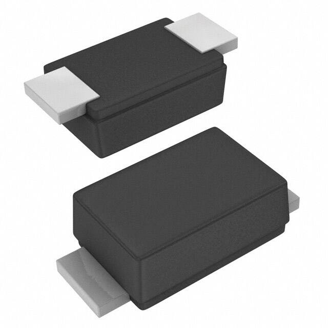
Top view
• Meets MSL level 1, per
LF maximum peak of 260 °C
Bottom view
• Wave and reflow solderable
SMF (DO-219AB)
Cathode
J-STD-020,
• AEC-Q101 qualified available
- Automotive ordering code: base P/NHM3
Anode
• Compatible to SOD-123W package case outline
• Material categorization: for definitions of compliance
please see www.vishay.com/doc?99912
LINKS TO ADDITIONAL RESOURCES
3D 3D
3D Models
TYPICAL APPLICATIONS
For use in high frequency inverters, freewheeling, DC/DC
converters, and polarity protection in commercial, industrial,
and automotive applications.
PRIMARY CHARACTERISTICS
IF(AV)
3.0 A
VRRM
100 V
IFSM
55 A
VF at IF = 3 A (TA = 125 °C)
0.62 V
TJ max.
175 °C
Package
SMF (DO-219AB)
Circuit configuration
Single
MECHANICAL DATA
Case: SMF (DO-219AB)
Molding compound meets UL 94 V-0 flammability rating
Base P/N-M3 - halogen-free, RoHS-compliant
Base P/NHM3 - halogen-free, RoHS-compliant, and
AEC-Q101 qualified
Terminals: matte tin plated leads, solderable per
J-STD-002 and JESD 22-B102
M3 and HM3 suffix meet JESD 201 class 2 whisker test
Polarity: color band denotes the cathode end
MAXIMUM RATINGS (TA = 25 °C unless otherwise noted)
PARAMETER
SYMBOL
Device marking code
Maximum repetitive peak reverse voltage
V3FM10
3MB
VRRM
100
(1)
2.5
IF(AV) (2)
3.0
Peak forward surge current 8.3 ms single half sine-wave
superimposed on rated load
IFSM
55
Operating junction temperature range
TJ (3)
-40 to +175
Storage temperature range
TSTG
-55 to +175
Maximum average forward rectified current (fig.1)
UNIT
IF(AV)
V
A
A
°C
Notes
(1) Free air, mounted on FR4 PCB, 2 oz. standard footprint
(2) Mounted on FR4 PCB, 2 oz. 10 mm x 10 mm copper pad areas
(3) The heat generated must be less than the thermal conductivity from junction-to-ambient: dP /dT < 1/R
D
J
θJA
Revision: 13-May-2020
Document Number: 87566
1
For technical questions within your region: DiodesAmericas@vishay.com, DiodesAsia@vishay.com, DiodesEurope@vishay.com
THIS DOCUMENT IS SUBJECT TO CHANGE WITHOUT NOTICE. THE PRODUCTS DESCRIBED HEREIN AND THIS DOCUMENT
ARE SUBJECT TO SPECIFIC DISCLAIMERS, SET FORTH AT www.vishay.com/doc?91000
�V3FM10
www.vishay.com
Vishay General Semiconductor
ELECTRICAL CHARACTERISTICS (TA = 25 °C unless otherwise noted)
PARAMETER
TEST CONDITIONS
IF = 1.5 A
Instantaneous forward voltage
TYP.
MAX.
0.59
-
0.74
0.83
0.52
-
0.62
0.70
TA = 25 °C
0.7
-
TA = 125 °C
500
-
-
85
900
3000
240
-
TA = 25 °C
IF = 3.0 A
VF (1)
IF = 1.5 A
TA = 125 °C
IF = 3.0 A
VR = 70 V
Reverse current
IR (2)
TA = 25 °C
VR = 100 V
Typical junction capacitance
SYMBOL
TA = 125 °C
4.0 V, 1 MHz
CJ
UNIT
V
μA
pF
Notes
(1) Pulse test: 300 μs pulse width, 1 % duty cycle
(2) Pulse test: Pulse width ≤ 5 ms
THERMAL CHARACTERISTICS (TA = 25 °c unless otherwise noted)
PARAMETER
SYMBOL
RθJA
Typical thermal resistance
V3FM10
(1)(2)
UNIT
125
RθJM (3)
°C/W
22
Notes
(1) The heat generated must be less than the thermal conductivity from junction-to-ambient: dP /dT
很抱歉,暂时无法提供与“V3FM10HM3/H”相匹配的价格&库存,您可以联系我们找货
免费人工找货- 国内价格 香港价格
- 3000+1.211373000+0.15702
- 6000+1.103526000+0.14304
- 9000+1.048559000+0.13592
- 15000+0.9867815000+0.12791
- 21000+0.9501921000+0.12317
- 30000+0.9146330000+0.11856
- 国内价格 香港价格
- 1+5.372191+0.69634
- 10+3.3139210+0.42955
- 100+2.11466100+0.27410
- 500+1.59352500+0.20655
- 1000+1.425331000+0.18475
- 国内价格
- 1+1.12200
- 200+0.86020
- 1500+0.74800
- 3000+0.69630
- 国内价格 香港价格
- 3000+0.932813000+0.12091