VCNL4040
www.vishay.com
Vishay Semiconductors
Fully Integrated Proximity and Ambient Light Sensor with
Infrared Emitter, I2C Interface, and Interrupt Function
FEATURES
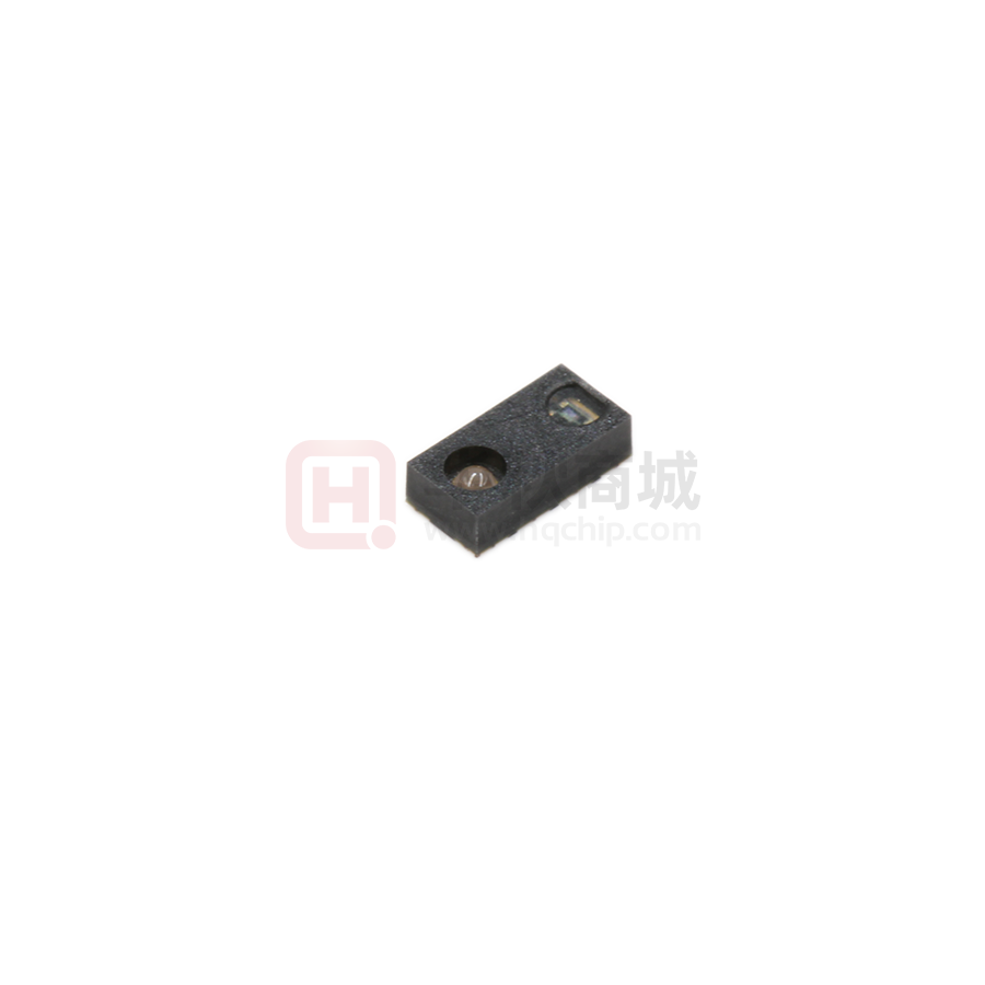
• Package type: surface mount
• Dimensions (L x W x H in mm): 4.0 x 2.0 x 1.1
• Integrated modules: infrared emitter (IRED),
ambient light sensor (ALS), proximity sensor
(PS), and signal conditioning IC
• Operates ALS and PS in parallel structure
• FiltronTM technology adoption
background light cancellation
for
robust
• Temperature compensation: -40 °C to +85 °C
DESCRIPTION
• Low power consumption I2C (SMBus compatible)
interface
VCNL4040 integrates a proximity sensor (PS), ambient
light sensor (ALS), and a high power IRED into one small
package. It incorporates photodiodes, amplifiers, and
analog to digital converting circuits into a single chip by
CMOS process. The 16-bit high resolution ALS offers
excellent sensing capabilities with sufficient selections to
fulfill most applications whether dark or high transparency
lens design. High and low interrupt thresholds can be
programmed for both ALS and PS, allowing the component
to use a minimal amount of the microcontrollers resources.
• Floor life: 168 h, MSL 3, according to J-STD-020
The proximity sensor features an intelligent cancellation
scheme, so that cross talk phenomenon is eliminated
effectively. To accelerate the PS response time, smart
persistence prevents the misjudgment of proximity sensing
but also keeps a fast response time. In active force mode, a
single measurement can be requested, allowing another
good approach for more design flexibility to fulfill different
kinds of applications with more power saving.
• Intelligent cancellation to reduce cross talk phenomenon
The patented FiltronTM technology achieves ambient light
spectral sensitivity closest to real human eye response and
offers the best background light cancellation capability
(including sunlight) without utilizing the microcontrollers’
resources. VCNL4040 provides an excellent temperature
compensation capability for keeping output stable under
various temperature configurations. ALS and PS functions
are easily set via the simple command format of I2C (SMBus
compatible) interface protocol. Operating voltage ranges
from 2.5 V to 3.6 V. VCNL4040 is packaged in a lead-free
8-pin molding package, which offers the best
market-proven reliability quality.
• Spectrum close to real human eye responses
• Output type: I2C bus (ALS / PS)
• Operation voltage: 2.5 V to 3.6 V
• Material categorization: for definitions of compliance
please see www.vishay.com/doc?99912
PROXIMITY FUNCTION
• Immunity to red glow (940 nm IRED)
• Programmable IRED sink current
• Smart persistence scheme to reduce PS response time
• Selectable for 12- / 16-bit PS output data
AMBIENT LIGHT FUNCTION
• High accuracy of ALS ±10 %
• Fluorescent light flicker immunity
• Selectable maximum detection range (819 / 1638 / 3277 /
6553) lux with highest sensitivity 0.0125 lux/step
INTERRUPT
• Programmable interrupt function for ALS and PS with
upper and lower thresholds
• Adjustable persistence to prevent false triggers for ALS
and PS
APPLICATIONS
• Handheld device
• Notebook, tablet PC
• Consumer device
• Industrial application
Rev. 1.4, 02-Mar-15
Document Number: 84274
1
For technical questions, contact: sensorstechsupport@vishay.com
THIS DOCUMENT IS SUBJECT TO CHANGE WITHOUT NOTICE. THE PRODUCTS DESCRIBED HEREIN AND THIS DOCUMENT
ARE SUBJECT TO SPECIFIC DISCLAIMERS, SET FORTH AT www.vishay.com/doc?91000
�VCNL4040
www.vishay.com
Vishay Semiconductors
PRODUCT SUMMARY
PART
NUMBER
OPERATING
RANGE
(mm)
VCNL4040
0 to 200
OPERATING I2C BUS
IRED PULSE
VOLTAGE VOLTAGE
CURRENT (1)
RANGE
RANGE
(mA)
(V)
(V)
2.5 to 3.6
1.8 to 3.6
200
AMBIENT
LIGHT
RANGE
(lx)
0.0125 to 6553
AMBIENT
ADC RESOLUTION
LIGHT
OUTPUT
PROXIMITY /
RESOLUTION
CODE
AMBIENT LIGHT
(lx)
0.0125
16 bit, I2C
16 bit / 16 bit
Note
(1) Adjustable through I2C interface
ORDERING INFORMATION
ORDERING CODE
VOLUME (1)
REMARKS
MOQ: 2500 pcs
4.0 mm x 2.0 mm x 1.1 mm
PACKAGING
VCNL4040M3OE
VCNL4040M3OE-H3
Tape and reel
4.34 mm x 2.35 mm x 3.25 mm
MOQ: 1500 pcs
VCNL4040M3OE-H5
4.34 mm x 2.35 mm x 3.65 mm
Note
(1) MOQ: minimum order quantity
ABSOLUTE MAXIMUM RATINGS (Tamb = 25 °C, unless otherwise specified)
PARAMETER
SYMBOL
MIN.
MAX.
Supply voltage
TEST CONDITION
VDD
2.5
3.6
UNIT
V
Operation temperature range
Tamb
-40
+85
°C
Storage temperature range
Tstg
-40
+100
°C
RECOMMENDED OPERATING CONDITIONS (Tamb = 25 °C, unless otherwise specified)
PARAMETER
TEST CONDITION
SYMBOL
MIN.
MAX.
UNIT
Supply voltage
VDD
2.5
3.6
V
Operation temperature range
Tamb
-40
+85
°C
I2C bus operating frequency
f(I2CCLK)
10
400
kHz
PIN DESCRIPTIONS
PIN ASSIGNMENT
SYMBOL
TYPE
1
GND
I
FUNCTION
Ground
2
CATHODE
I
Cathode (sensor) connection
3
VDD
I
Power supply input
4
ANODE
I
Anode for IRED
5
CATHODE
I
Cathode (LED) connection
6
INT
O
Interrupt pin
7
SDAT
I / O (open drain)
I2C data bus data input / output
8
SCLK
I
I2C digital bus clock input
Rev. 1.4, 02-Mar-15
Document Number: 84274
2
For technical questions, contact: sensorstechsupport@vishay.com
THIS DOCUMENT IS SUBJECT TO CHANGE WITHOUT NOTICE. THE PRODUCTS DESCRIBED HEREIN AND THIS DOCUMENT
ARE SUBJECT TO SPECIFIC DISCLAIMERS, SET FORTH AT www.vishay.com/doc?91000
�VCNL4040
www.vishay.com
Vishay Semiconductors
BLOCK DIAGRAM
VDD
Anode
PD Timing
Controller
PD
Buffer
DSP
IR LED
PS
PD
Oscillator
INT
SCLK
SDAT
LED Driver
LED_CATHODE
Temperature
Sensor
I2C Bus Logic
Control
ALS
PD
ALS
16 bits
Data
Buffer
Low Pass Filter
GND
BASIC CHARACTERISTICS (Tamb = 25 °C, unless otherwise specified)
PARAMETER
TEST CONDITION
Supply voltage
Excluded LED driving
Supply current
Light condition = dark, VDD = 3.3 V
I2C supply voltage
MIN.
VDD
2.5
IDD
PS shut down
Logic high
Logic low
Logic high
Logic low
ALS disable, PS enable
IALSSD
ALS enable, PS disable
IPSSD
VDD = 3.3 V
VDD = 2.6 V
Peak sensitivity wavelength of
ALS
Peak sensitivity wavelength of PS
VIH
TYP.
3.6
UNIT
V
μA
0.2
1.8
μA
3.6
V
200
μA
260
μA
1.55
0.4
VIL
VIH
MAX.
300
IDD (SD)
VPULL UP
ALS shut down
I2C signal input
SYMBOL
1.4
0.4
VIL
λp
550
λpps
940
V
V
nm
nm
Full ALS counts
16-bit resolution
65 535
steps
Full PS counts
12-bit / 16-bit resolution
4096 / 65 535
steps
White LED light source
± 10
%
ALS sensing tolerance
Detectable
intensity
Minimum
IT = 640 ms, 1 step (1)(2)
0.0125
Maximum
IT = 80 ms, 65 535 step (1)(2)
6553
ALS dark offset
PS detection range
IT = 80 ms, normal sensitivity (1)
0
3
steps
Kodak white card
0
200
mm
-40
+85
°C
2.5
3.6
V
200
mA
Operating temperature range
Tamb
Cathode (sensor) voltage
IRED driving current
lx
(3)
Notes
(1) Test condition: V
DD = 3.3 V, temperature: 25 °C
(2) Maximum detection range to ambient light can be determined by ALS refresh time adjustment. Refer to table “ALS Resolution and Maximum
Detection Range”
(3) Based on IRED on / off duty ratio = 1/40, 1/80, 1/160, and 1/320
Rev. 1.4, 02-Mar-15
Document Number: 84274
3
For technical questions, contact: sensorstechsupport@vishay.com
THIS DOCUMENT IS SUBJECT TO CHANGE WITHOUT NOTICE. THE PRODUCTS DESCRIBED HEREIN AND THIS DOCUMENT
ARE SUBJECT TO SPECIFIC DISCLAIMERS, SET FORTH AT www.vishay.com/doc?91000
�VCNL4040
www.vishay.com
Vishay Semiconductors
I2C BUS TIMING CHARACTERISTICS (Tamb = 25 °C, unless otherwise specified)
PARAMETER
SYMBOL
Clock frequency
STANDARD MODE
FAST MODE
MAX.
f(SMBCLK)
10
100
t(BUF)
4.7
1.3
μs
t(HDSTA)
4.0
0.6
μs
Repeated start condition setup time
t(SUSTA)
4.7
0.6
μs
Stop condition setup time
t(SUSTO)
4.0
0.6
Data hold time
t(HDDAT)
Data setup time
Bus free time between start and stop condition
Hold time after (repeated) start condition;
after this period, the first clock is generated
MIN.
MAX.
10
400
UNIT
MIN.
3450
kHz
μs
900
ns
t(SUDAT)
250
100
ns
I2C clock (SCK) low period
t(LOW)
4.7
1.3
μs
I2C clock (SCK) high period
t(HIGH)
4.0
0.6
μs
Clock / data fall time
t(F)
300
300
ns
Clock / data rise time
t(R)
1000
300
ns
t(LOW)
I2C bus
CLOCK
(SCLK)
t(R)
t(F)
VIH
VIL
t(HDSTA)
t(SUSTO)
t(BUF)
t(HDDAT)
I2C bus
DATA
(SDAT)
t(SUDAT)
VIH
VIL
{
P
Stop Condition
t(SUSTA)
t(HIGH)
{
{
S
Star Condition
{
S
Start
P
Stop
t(LOSEXT)
SCLKACK
t(LOWMEXT)
SDAACK
t(LOWMEXT)
t(LOWMEXT)
2
I C bus
CLOCK
(SCLK)
I2C bus
DATA
(SDAT)
Fig. 1 - I2C Bus Timing Diagram
Rev. 1.4, 02-Mar-15
Document Number: 84274
4
For technical questions, contact: sensorstechsupport@vishay.com
THIS DOCUMENT IS SUBJECT TO CHANGE WITHOUT NOTICE. THE PRODUCTS DESCRIBED HEREIN AND THIS DOCUMENT
ARE SUBJECT TO SPECIFIC DISCLAIMERS, SET FORTH AT www.vishay.com/doc?91000
�VCNL4040
www.vishay.com
Vishay Semiconductors
PARAMETER TIMING INFORMATION
I2C bus
CLOCK
(SCLK)
I2C bus
DATA
(SDAT)
SA7
SA6
SA5
SA4
SA3
W
SA1
SA2
Start by
Master
SA7
SA6
SA5
SA4
SA3
SA0
SA1
SA2
ACK by
VCNL4040
ACK by
VCNL4040
I2CBus Slave Address Byte
Command Code
I2C bus
CLOCK
(SCLK)
I2C bus
DATA
(SDAT)
SA7
SA6
SA5
SA4
SA3
SA2
SA0
SA1
SA7
SA6
SA5
SA4
SA3
SA2
SA1
SA0
ACK by
VCNL4040
ACK by
VCNL4040
Data Byte Low
Stop by
Master
Data Byte High
Fig. 2 - I2C Bus Timing for Sending Word Command Format
I2CBus
CLOCK
(SCLK)
I2CBus
DATA
(SDAT)
SA7
SA6
SA5
SA4
SA3
W
SA1
SA2
Start by
Master
SA7
SA6
SA5
SA4
SA3
SA0
SA1
SA2
ACK by
VCNL4040
ACK by
VCNL4040
I2CBus Slave Address Byte
Command Code
I2CBus
CLOCK
(SCLK)
I2CBus
DATA
(SDAT)
SA6
SA7
SA5
SA4
SA3
SA2
R
SA1
Start by
Master
SA7
SA6
SA5
SA4
SA3
SA2
SA1
SA0
ACK by
Master
ACK by
VCNL4040
I2CBus Slave Address Byte
Data Byte Low
I2CBus
CLOCK
(SCLK)
I2CBus
DATA
(SDAT)
SA7
SA6
SA5
SA4
SA3
SA2
SA1
SA0
ACK by
Master
Stop by
Master
Data Byte High
Fig. 3 - I2C Bus Timing for Receiving Word Command Format
Rev. 1.4, 02-Mar-15
Document Number: 84274
5
For technical questions, contact: sensorstechsupport@vishay.com
THIS DOCUMENT IS SUBJECT TO CHANGE WITHOUT NOTICE. THE PRODUCTS DESCRIBED HEREIN AND THIS DOCUMENT
ARE SUBJECT TO SPECIFIC DISCLAIMERS, SET FORTH AT www.vishay.com/doc?91000
�VCNL4040
www.vishay.com
Vishay Semiconductors
TYPICAL PERFORMANCE CHARACTERISTICS (Tamb = 25 °C, unless otherwise specified)
Axis Title
100
10000
PS-CH
ALS-CH
80
70
1000
60
1st line
2nd line
2nd line
Normalized Output (%)
90
50
40
100
30
20
10
0
400
500
600
700
800
900
10
1000
λ - Wavelength (nm)
2nd line
Fig. 4 - Normalized Spectral Response
Fig. 7 - IDD vs.Temperature
Fig. 5 - Forward Current IF = f (VF)
Fig. 8 - ALS View Angle
Axis Title
Axis Title
70 000
10000
1.0
160 ms
60 000
10000
0.9
40 000
320 ms
30 000
640 ms
100
20 000
0.7
1000
0.6
1st line
2nd line
1000
1st line
2nd line
Step
1st line
80 ms
Normalized Output
1st line
0.8
50 000
0.5
0.4
100
0.3
0.2
10 000
0.1
0
0
2000
4000
6000
8000
10
10 000
0
400
500
600
700
800
900
10
1000
Lux
2nd line
Wavelength (nm)
2nd line
Fig. 6 - ALS Refresh Time vs. Maximum Detection Range
Fig. 9 - White Channel Spectral Response
Rev. 1.4, 02-Mar-15
Document Number: 84274
6
For technical questions, contact: sensorstechsupport@vishay.com
THIS DOCUMENT IS SUBJECT TO CHANGE WITHOUT NOTICE. THE PRODUCTS DESCRIBED HEREIN AND THIS DOCUMENT
ARE SUBJECT TO SPECIFIC DISCLAIMERS, SET FORTH AT www.vishay.com/doc?91000
�VCNL4040
www.vishay.com
Vishay Semiconductors
Fig. 10 - IRED Profile
APPLICATION INFORMATION
Pin Connection with the Host
VCNL4040 integrates proximity sensor, ambient light Sensor, and IRED all together with I2C interface. It is very easy for the
baseband (CPU) to access PS and ALS output data via I2C interface without extra software algorithms. The hardware schematic
is shown in the following diagram.
Two additional capacitors in the circuit can be used for the following purposes: (1) the 0.1 μF capacitor near the VDD pin is used
for power supply noise rejection, (2) the 2.2 μF capacitor - connected to the anode - is used to prevent the IRED voltage from
instantly dropping when the IRED is turned on, and (3) 2.2 kΩ is suitable for the pull up resistor of I2C except for the 8.2 kΩ
applied on the INT pin.
Note
• Cathode (LED) and cathode (sensor): pins need to be connected together externally
VPull_up
VDD
VDD_LED
0.1uF
2.2KΩ
2.2uF
2.2KΩ
3
8
4
SCLK
SCK
Anode
7
SDA
SDAT
8.2KΩ
VCNL4040
Baseband
INT
6
CATHODE
(LED)
5
INT
GND
CATHODE
(Sensor)
2
1
Fig. 11 - Hardware Pin Connection Diagram
Rev. 1.4, 02-Mar-15
Document Number: 84274
7
For technical questions, contact: sensorstechsupport@vishay.com
THIS DOCUMENT IS SUBJECT TO CHANGE WITHOUT NOTICE. THE PRODUCTS DESCRIBED HEREIN AND THIS DOCUMENT
ARE SUBJECT TO SPECIFIC DISCLAIMERS, SET FORTH AT www.vishay.com/doc?91000
�VCNL4040
www.vishay.com
Vishay Semiconductors
Digital Interface
VCNL4040 applies single slave address 0x60 (HEX) of 7-bit addressing following I2C protocol. As figure 12 shows, VCNL4040’s
I2C command format is simple for read and write operations between VCNL4040 and the host. The white sections indicate host
activity and the gray sections indicate VCNL4040’s acknowledgement of the host access activity. Write word and read word
protocol is suitable for accessing registers particularly for 16-bit data ALS and 12-bit / 16-bit PS data. Interrupt can be cleared
by reading data out from register: INT_Flag. All command codes should follow read word and write word protocols.
Send Byte ɦ Write Command to VCNL4040
1
S
1
1
8
1
8
1
8
1
1
Wr
A
Command Code
A
Data Byte Low
A
Data Byte High
A
P
7
Slave Address
Receive Byte ɦ Read Data from VCNL4040
1
7
1
1
8
1
1
7
1
1
8
1
8
1
1
S
Slave Address
Wr
A
Command Code
A
S
Slave Address
Rd
A
Data Byte Low
A
Data Byte High
A
P
S = start condition
P = stop condition
A = acknowledge
Shaded area = VCNL4040 acknowledge
Fig. 12 - Write Word and Read Word Protocol
Function Description
VCNL4040 applies a 16-bit high resolution ALS that provides the best ambient light sensing capability down to 0.01 lux/step
which works well under a low transmittance lens design (dark lens). A flexible interrupt function of ALS (register: ALS_CONF)
is also supported. The INT signal will not be triggered by VCNL4040 if the ALS value is not over high INT threshold window level,
or lower than low INT threshold window level of ALS. VCNL4040 detects different light sources such as fluorescent light,
incandescent light, sunlight, and white LED with high accuracy ALS data output after detecting algorithm is implemented.
For proximity sensor function, VCNL4040 supports different kinds of mechanical designs to achieve the best proximity detection
performance for any color of object with more flexibility. The basic PS function settings, such as duty ratio, integration time,
interrupt, and PS enable / disable, and persistence, are handled by the register: PS_CONF1. Duty ratio controls the PS response
time. Integration time represents the duration of the energy being received. The interrupt is triggered when the PS detection
levels over the high threshold level setting (register: PS_THDH) or lower than low threshold (register: PS_THDL). If the interrupt
function is enabled, the host can react to the interrupt pin, instead of polling the PS data registers. The INT flag (register:
INT_Flag) indicates the type of interrupt that has been triggered, depending on the interrupt settings in the configuration
registers. PS persistence (PS_PERS) sets up the PS INT trigger conditions, defining the amount of consecutive hits required
before an interrupt event occurs. The intelligent cancellation level can be set on register: PS_CANC to reduce the cross talk
phenomenon.
VCNL4040 also supports an easy to use proximity detection logic mode, that triggers when the PS high threshold is exceeded
and automatically resets the interrupt pin when the proximity reading falls beneath the PS low threshold. This functionality can
be set in the register: PS_MS. A smart persistence is provided to be able to prevent false PS interrupt trigger events.
Descriptions of each of these parameters are shown in table 1.
Rev. 1.4, 02-Mar-15
Document Number: 84274
8
For technical questions, contact: sensorstechsupport@vishay.com
THIS DOCUMENT IS SUBJECT TO CHANGE WITHOUT NOTICE. THE PRODUCTS DESCRIBED HEREIN AND THIS DOCUMENT
ARE SUBJECT TO SPECIFIC DISCLAIMERS, SET FORTH AT www.vishay.com/doc?91000
�VCNL4040
www.vishay.com
Vishay Semiconductors
TABLE 1 - COMMAND CODE AND REGISTER DESCRIPTION
COMMAND DATE BYTE
CODE
LOW / HIGH
0x00
0x01
0x02
0x03
0x04
0x05
0x06
0x07
0x08
0x09
0x0A
0x0B
0x0C
REGISTER
NAME
R/W
DEFAULT
VALUE
FUNCTION DESCRIPTION
L
ALS_CONF
R/W
0x01
ALS integration time, persistence, interrupt, and function enable / disable
H
Reserved
R/W
0x00
Reserved
L
ALS_THDH_L R / W
0x00
ALS high interrupt threshold LSB byte
H
ALS_THDH_M R / W
0x00
ALS high interrupt threshold MSB byte
L
ALS_THDL_L R / W
0x00
ALS low interrupt threshold LSB byte
H
ALS_THDL_M R / W
0x00
ALS low interrupt threshold MSB byte
L
PS_CONF1
0x01
PS duty ratio, integration time, persistence, and PS enable / disable
H
PS_CONF2
R/W
0x00
PS output resolution selection, PS interrupt trigger method
L
PS_CONF3
R/W
0x00
PS smart persistence, active force mode
H
PS_MS
R/W
0x00
White channel enable / disable, PS mode selection, PS protection setting,
and LED current selection
R/W
L
PS_CANC_L
R/W
0x00
PS cancellation level setting
H
PS_CANC_M R / W
0x00
PS cancellation level setting
L
PS_THDL_L
0x00
PS low interrupt threshold setting LSB byte
R/W
H
PS_THDL_M
R/W
0x00
PS low interrupt threshold setting MSB byte
L
PS_THDH_L
R/W
0x00
PS high interrupt threshold setting LSB byte
H
PS_THDH_M
R/W
0x00
PS high interrupt threshold setting MSB byte
L
PS_Data_L
R
0x00
PS LSB output data
H
PS_Data_M
R
0x00
PS MSB output data
L
ALS_Data_L
R
0x00
ALS LSB output data
H
ALS_Data_M
R
0x00
ALS MSB output data
L
White_Data_L
R
0x00
White LSB output data
H
White_Data_M
R
0x00
White MSB output data
L
Reserved
R
0x00
Reserved
H
INT_Flag
R
0x00
ALS, PS interrupt flags
L
ID_L
R
0x86
Device ID LSB
H
ID_M
R
0x01
Device ID MSB
Note
• All of reserved register are used for internal test. Please keep as default setting.
Command Register Format
VCNL4040 provides an 8-bit command register for ALS and PS controlling independently. The description of each command
format is shown in following tables.
TABLE 2 - REGISTER: ALS_CONF DESCRIPTION
REGISTER NAME
Command
COMMAND CODE: 0x00_L (0x00 DATA BYTE LOW)
Bit
7
REGISTER: ALS_CONF
Command
6
5
Bit
3
1
0
Description
7:6
Reserved
5:4
Default = (0 : 0)
3:2
(0 : 0) = 1, (0 : 1) = 2, (1 : 0) = 4, (1 : 1) = 8
ALS interrupt persistence setting
ALS_INT_EN
1
0 = ALS interrupt disable, 1 = ALS interrupt enable
ALS_SD
0
0 = ALS power on, 1 = ALS shut down, default = 1
Rev. 1.4, 02-Mar-15
2
(0 : 0) = 80 ms; (0 : 1) = 160 ms; (1 : 0) = 320 ms; (1 : 1) = 640 ms
ALS integration time setting, longer integration time has higher sensitivity
ALS_IT
ALS_PERS
4
COMMAND CODE: 0x00_L (0x00 DATA BYTE LOW)
Document Number: 84274
9
For technical questions, contact: sensorstechsupport@vishay.com
THIS DOCUMENT IS SUBJECT TO CHANGE WITHOUT NOTICE. THE PRODUCTS DESCRIBED HEREIN AND THIS DOCUMENT
ARE SUBJECT TO SPECIFIC DISCLAIMERS, SET FORTH AT www.vishay.com/doc?91000
�VCNL4040
www.vishay.com
Vishay Semiconductors
TABLE 3 - REGISTER: 00H_H DESCRIPTION
REGISTER: Reserved
COMMAND CODE: 0x00_H (0x00 DATA BYTE HIGH)
Command
Bit
Reserved
7:0
Description
Default = (0 : 0 : 0 : 0 : 0 : 0 : 0 : 0)
TABLE 4 - REGISTER ALS_THDH_L AND ALS_THDH_M DESCRIPTION
COMMAND CODE: 0x01_L (0x01 DATA BYTE LOW) OR 0x01_H (0x01 DATA BYTE HIGH)
Register
Bit
Description
ALS_THDH_L
7:0
0x00 to 0xFF, ALS high interrupt threshold LSB byte
ALS_THDH_M
7:0
0x00 to 0xFF, ALS high interrupt threshold MSB byte
TABLE 5 - REGISTER: ALS_THDL_L AND ALS_THDL_M DESCRIPTION
COMMAND CODE: 0x02_L (0x02 DATA BYTE LOW) AND 0x02_H(0x02 DATA BYTE HIGH)
Register
Bit
Description
ALS_THDL_L
7:0
0x00 to 0xFF, ALS low interrupt threshold LSB byte
ALS_THDL_M
7:0
0x00 to 0xFF, ALS low interrupt threshold MSB byte
TABLE 6 - REGISTER: PS_CONF1 DESCRIPTION
REGISTER: PS_CONF1
Command
COMMAND CODE: 0x03_L (0x03 DATA BYTE LOW)
Bit
Description
PS_Duty
7:6
(0 : 0) = 1/40, (0 : 1) = 1/80, (1 : 0) = 1/160, (1 : 1) = 1/320
PS IRED on / off duty ratio setting
PS_PERS
5:4
(0 : 0) = 1, (0 : 1) = 2, (1 : 0) = 3, (1 : 1) = 4
PS interrupt persistence setting
PS_ IT
3:1
(0 : 0 : 0) = 1T, (0 : 0 : 1) = 1.5T, (0 : 1 : 0) = 2T, (0 : 1 : 1) = 2.5T, (1 : 0 : 0) = 3T, (1 : 0 : 1) = 3.5T,
(1 : 1 : 0) = 4T, (1 : 1 : 1) = 8T, PS integration time setting
PS_SD
0
0 = PS power on, 1 = PS shut down, default = 1
TABLE 7 - REGISTER: PS_CONF2 DESCRIPTION
REGISTER: PS_CONF2
COMMAND CODE: 0x03_H (0x03 DATA BYTE HIGH)
Command
Bit
Reserved
7:6
(0 : 0), reserved
Description
Reserved
5:4
(0 : 0), reserved
PS_HD
3
0 = PS output is 12 bits; 1 = PS output is 16 bits
Reserved
2
Default = 0
PS_INT
1:0
(0 : 0) = interrupt disable, (0 : 1) = trigger when close, (1 : 0)= trigger when away,
(1 : 1)= trigger when close or away
TABLE 8 - REGISTER: PS_CONF3 DESCRIPTION
REGISTER: PS_CONF3
COMMAND CODE: 0x04_L (0x04 DATA BYTE LOW)
Command
Bit
Reserved
7
Reserved
6:5
Description
0
(0 : 0)
PS_SMART_PERS
4
0 = disable; 1 = enable PS smart persistence
PS_AF
3
0 = active force mode disable (normal mode), 1 = active force mode enable
PS_TRIG
2
0 = no PS active force mode trigger, 1 = trigger one time cycle
VCNL4040 output one cycle data every time host writes in ‘1’ to sensor.
The state returns to ‘0’ automatically.
Reserved
1:0
Rev. 1.4, 02-Mar-15
(0 : 0)
Document Number: 84274
10
For technical questions, contact: sensorstechsupport@vishay.com
THIS DOCUMENT IS SUBJECT TO CHANGE WITHOUT NOTICE. THE PRODUCTS DESCRIBED HEREIN AND THIS DOCUMENT
ARE SUBJECT TO SPECIFIC DISCLAIMERS, SET FORTH AT www.vishay.com/doc?91000
�VCNL4040
www.vishay.com
Vishay Semiconductors
TABLE 9 - REGISTER: PS_MS DESCRIPTION
REGISTER: PS_MS
COMMAND CODE: 0x04_H (0x04 DATA BYTE HIGH)
Command
Bit
White_EN
7
0 = white channel enabled
1 = white channel disabled
PS_MS
6
0 = proximity normal operation with interrupt function
1 = proximity detection logic output mode enable
Reserved
LED_I
Description
5:3
(0:0:0)
2:0
(0 : 0 : 0) = 50 mA; (0 : 0 : 1) = 75 mA; (0 : 1 : 0) = 100 mA; (0 : 1 : 1) = 120 mA
(1 : 0 : 0) = 140 mA; (1 : 0 : 1) = 160 mA; (1 : 1 : 0) = 180 mA; (1 : 1 : 1) = 200 mA
LED current selection setting
TABLE 10 - REGISTER PS_CANC_L AND PS_CANC_M DESCRIPTION
COMMAND CODE: 0x05_L (0x05 DATA BYTE LOW) AND 0x05_H(0x05 DATA BYTE HIGH)
Register
Bit
Description
PS_CANC_L
7:0
0x00 to 0xFF, PS cancellation level setting_LSB byte
PS_CANC_M
7:0
0x00 to 0xFF, PS cancellation level setting_MSB byte
TABLE 11 - REGISTER: PS_THDL_L AND PS_THDL_M DESCRIPTION
COMMAND CODE: 0x06_L (0x06 DATA BYTE LOW) AND 0x06_H(0x06 DATA BYTE HIGH)
Register
Bit
Description
PS_THDL_L
7:0
0x00 to 0xFF, PS interrupt low threshold setting_LSB byte
PS_THDL_M
7:0
0x00 to 0xFF, PS interrupt low threshold setting_MSB byte
TABLE 12 - REGISTER: PS_THDH_L AND PS_THDH_M DESCRIPTION
COMMAND CODE: 0x07_L (0x07 DATA BYTE LOW) AND 0x07_H(0x07 DATA BYTE HIGH)
Register
Bit
Description
PS_THDH_L
7:0
0x00 to 0xFF, PS interrupt high threshold setting_LSB byte
PS_THDH_M
7:0
0x00 to 0xFF, PS interrupt high threshold setting_MSB byte
TABLE 13 - READ OUT REGISTER DESCRIPTION
Register
PS_Data_L
Command Code
Bit
Description
0x08_L (0x08 data byte low)
7:0
PS_Data_M
0x08_H (0x08 data byte high)
7:0
0x00 to 0xFF, PS MSB output data
ALS_Data_L
0x09_L (0x09 data byte low)
7:0
0x00 to 0xFF, ALS LSB output data
ALS_Data_M
0x09_H (0x09 data byte high)
7:0
0x00 to 0xFF, ALS MSB output data
White_Data_L
0x0A_L (0x0A data byte low)
7:0
0x00 to 0xFF, white LSB output data
White_Data_M
0x0A_H (0x0A data byte high)
7:0
0x00 to 0xFF, white LSB output data
Reserved
0x0B_L (0x0B data byte low)
7:0
INT_Flag
0x0B_H (0x0B data byte high)
7
6
5
4
3
2
1
0
ID_L
0CH_L (0CH data byte low)
7:0
86H for MP version sample, device ID LSB byte
0CH_H (0CH data byte high)
7:6
5:4
3:0
(0 : 0)
(0 : 0) Slave address = 0x60 (7-bit)
Version code (0 : 0 : 0 : 1), device ID MSB byte
ID_M
Rev. 1.4, 02-Mar-15
0x00 to 0xFF, PS LSB output data
Default = 0x00
Reserved
PS_SPFLAG, PS entering protection mode
ALS_IF_L, ALS crossing low THD INT trigger event
ALS_IF_H, ALS crossing high THD INT trigger event
Reserved
Reserved
PS_IF_CLOSE, PS rises above PS_THDH INT trigger event
PS_IF_AWAY, PS drops below PS_THDL INT trigger event
Document Number: 84274
11
For technical questions, contact: sensorstechsupport@vishay.com
THIS DOCUMENT IS SUBJECT TO CHANGE WITHOUT NOTICE. THE PRODUCTS DESCRIBED HEREIN AND THIS DOCUMENT
ARE SUBJECT TO SPECIFIC DISCLAIMERS, SET FORTH AT www.vishay.com/doc?91000
�VCNL4040
www.vishay.com
Vishay Semiconductors
Adjustable Sampling Time
VCNL4040’s LED driver drives the internal IRED with the “LED CATHODE” pin by a pulsed duty cycle. The IRED on / off duty
ratio can be set in register: PS_Duty which is related to the current consumption and PS response time. The higher the duty
ratio, the faster the response time achieved with higher power consumption. For example, PS_Duty = 1/320, peak IRED current
= 100 mA, averaged current consumption is 100 mA/320 = 0.3125 mA.
Initialization
VCNL4040 includes default values for each register. As long as power is on, it is ready to be controlled by host via I2C bus.
Threshold Window Setting
• ALS Threshold Window Setting (Applying ALS INT)
Register: ALS_THDH_L and ALS_THDH_M defines 16-bit ALS high threshold data for LSB byte and MSB byte. Register:
ALS_THDL_L and ALS_THDL_M defines 16-bit ALS low threshold data for LSB byte and MSB byte. As long as ALS INT
function is enabled, INT will be triggered once the ALS data exceeds ALS_THDH or goes below ALS_THDL. To easily define
the threshold range, multiply the value of the resolution (lux/step) by the threshold level (refer to table 14).
TABLE 14 - ALS RESOLUTION AND MAXIMUM DETECTION RANGE
ALS_IT
ALS_IT
(7 : 6)
SENSITIVITY
MAXIMUM DETECTION
RANGE
UNIT
(lux/step)
UNIT
(lux)
INTEGRATION TIME
(typ.)
(0, 0)
80 ms
0.10
6553.5
(0, 1)
160 ms
0.05
3276.8
(1, 0)
320 ms
0.025
1638.4
(1, 1)
640 ms
0.0125
819.2
• ALS Persistence
The ALS INT is triggered once the ALS value is higher or lower than the threshold window. The ALS_PERS (1, 2, 4,
parameter, sets the amount of consecutive hits needed, in order for an interrupt event to trigger.
8 times)
• Programmable PS Threshold
VCNL4040 provides both high and low thresholds setting for PS (register: PS_THDL, PS_THDH).
• PS Persistence
The PS persistence function (PS_PERS, 1, 2, 3, 4) helps to avoid false trigger of the PS INT. It defines the amount of
consecutive hits needed in order for a PS interrupt event to be triggered.
• PS Active Force mode
An extreme power saving way to use PS is to apply PS active force (register: PS_CONF3 command: PS_AF = 1) mode.
Anytime host would like to request one proximity measurement, write a ‘1’ into register: PS_CONF3 command: PS_Trig. This
triggers a single PS measurement, which can be read from the PS result registers. VCNL4040 stays in standby mode
constantly.
Data Access
All of VCNL4040 16 bit command registers are readable. The result data for ALS, white, and PS measurements can be read out
form their respective registers. Each result is made of 2 bytes.
TABLE 15 - 16-BIT ALS DATA FORMAT
VCNL4040
Bit
15
14
Register
13
12
11
ALS_DataM
10
9
8
7
6
5
4
3
2
1
0
ALS_DataL
Intelligent Cancellation
VCNL4040 provides an intelligent cancellation method to reduce cross talk phenomenon for the proximity sensor. The output
data will be subtracted by the value set in register: PS_CANC.
Rev. 1.4, 02-Mar-15
Document Number: 84274
12
For technical questions, contact: sensorstechsupport@vishay.com
THIS DOCUMENT IS SUBJECT TO CHANGE WITHOUT NOTICE. THE PRODUCTS DESCRIBED HEREIN AND THIS DOCUMENT
ARE SUBJECT TO SPECIFIC DISCLAIMERS, SET FORTH AT www.vishay.com/doc?91000
�VCNL4040
www.vishay.com
Vishay Semiconductors
Interruption (INT)
The VCNL4040 has an interrupt feature for both the PS and ALS channel. The purpose of the interrupt feature is to actively
inform the host once INT has been triggered. When the interrupt is enabled, the host does not need to continuously read the
data registers of the sensor, but instead can simply react to the interrupt pin. As long as the host enables ALS interrupt (register:
ALS_INT_EN) or PS interrupt (register: PS_INT) function, the level of INT pin (pin 6) is pulled low once an interrupt event has
been triggered. All registers are accessible even if INT is triggered.
ALS INT is triggered when ALS value crosses over the value set in register: ALS_THDH or below the value set by
register: ALS_THDL. PS INT is triggered when the PS value crosses over the value set in register: PS_THDH or falls below the
value set in register: PS_THDL. Which of these thresholds to react to, can be set by the PS_INT bits in the register: PS_CONF2.
Interruption Flag
Register: INT_Flag represents all of the interrupt trigger statuses for ALS and PS. If any of these flags trigger from “0” to “1”,
the INT pin will be pulled low. Once the host reads INT_Flag register, all the flags are cleared (reset to "0"), and the INT pin is
reset to high.
PROXIMITY DETECTION LOGIC OUTPUT MODE
VCNL4040 has a proximity detection logic mode, enabling the host to read the state of PS (near or far) simply by monitoring the
INT pin (pin 6). When this mode is selected, the INT pin is pulled low when an object is close to the sensor (value is above high
threshold) and is reset to high when the object moves away (value is below low threshold). Register: PS_THDH / PS_THDL
define where these threshold levels are set.
It should be noted that whenever the proximity detection logic mode has been enabled, the INT pin only reacts to proximity
interrupt events. If the host would like to use ALS INT function, the bit PS_MS in the register: PS_MS needs to be set to normal
operation mode (PS_MS = 0). In order for the proximity detection logic mode to function, one of the PS_INT bits in register:
PS_CONF2 must be enabled (“trigger when close”, “trigger when away”, or “trigger when close or away”). If PS_INT is set to
“INT Disable” the proximity detection logic mode will not function.
PROXIMITY DETECTION HYSTERESIS
A hysteresis is created by setting the low and high threshold values. With proximity detection logic mode disabled, an interrupt
event will trigger and stay triggered until it is cleared in the INT_Flag register. The register is cleared automatically once it is read.
If the interrupt flags are not cleared after an interrupt event has occurred, the VCNL4040 will not react to another interrupt event
until the INT-Flag register has been cleared. An example of this could be when turning on and off a backlight of a mobile display.
First the PS INT triggers when the PS value is over PS_THDH. The host switches off the panel backlight and then clears INT.
When PS value is less than PS_THDL, host switches on panel backlight.
VPull_up
VDD
VDD_LED
0.1uF
2.2KΩ
2.2uF
2.2KΩ
3
8
SCK
4
SCLK
Anode
7
SDA
SDAT
8.2KΩ
VCNL4040
Baseband
GPIO
6
CATHODE
(LED)
5
INT
GND
CATHODE
(Sensor)
2
1
Fig. 13 - VCNL4040 Reference Circuit Connection with Host (Proximity Detection Logic Output Mode)
(VCNL4040 INT pin connecting to BB GPIO instead of INT pin)
Rev. 1.4, 02-Mar-15
Document Number: 84274
13
For technical questions, contact: sensorstechsupport@vishay.com
THIS DOCUMENT IS SUBJECT TO CHANGE WITHOUT NOTICE. THE PRODUCTS DESCRIBED HEREIN AND THIS DOCUMENT
ARE SUBJECT TO SPECIFIC DISCLAIMERS, SET FORTH AT www.vishay.com/doc?91000
�VCNL4040
www.vishay.com
Vishay Semiconductors
PACKAGE INFORMATION (VCNL4040M3OE) in millimeters
Top View
Side View
Bottom View
1.1 ± 0.05
0.9
2 ± 0.1
4
4
5
0.675 x 8
Ø1.1
0.55
1.075
Sensor
1.075
Ø1.2
2.6
LED
1.45
4 ± 0.1
1.075
0.85
5
0.5
8
1
1
8
0.75
1
1
GND
2
Cathode
3
4
5
Cathode
(LED)
6
INT
VDD
7
SDAT
Anode
8
SCLK
(sensor)
Fig. 14 - VCNL4040 Package Dimensions
LAYOUT PAD INFORMATION (VCNL4040M3OE) in millimeters
Pad Center to Center
1.4
1.075
0.7
0.725 x 8
1.075
0.7 x 8
1.075
Pad Cente r to Center
0.35
Fig. 15 - VCNL4040M3OE PCB Layout Footprint
Rev. 1.4, 02-Mar-15
Document Number: 84274
14
For technical questions, contact: sensorstechsupport@vishay.com
THIS DOCUMENT IS SUBJECT TO CHANGE WITHOUT NOTICE. THE PRODUCTS DESCRIBED HEREIN AND THIS DOCUMENT
ARE SUBJECT TO SPECIFIC DISCLAIMERS, SET FORTH AT www.vishay.com/doc?91000
�VCNL4040
www.vishay.com
Vishay Semiconductors
PACKAGE INFORMATION (VCNL4040M3OE-H3) in millimeters
Top View
Side View
Bottom View
3.25 ± 0.2
0.8
2.35 ± 0.2
4
4
5
0.7(x8)
1.075
2.6
4.34 ± 0.2
1.075
1.02
5
Ø1.2
1.075
Ø1.1
8
1
1
8
1
1
GND
5
Cathode
Cathode
(LED)
6
INT
3
VDD
7
SDAT
4
Anode
8
SCLK
2
(sensor)
0.575
Fig. 16 - VCNL4040M3OE-H3 Package Dimensions
PACKAGE INFORMATION (VCNL4040M3OE-H5) in millimeters
Top View
Side View
Bottom View
3.65 ± 0.2
0.8
2.35 ± 0.2
4
4
5
0.7(x8)
1.075
2.6
4.34 ± 0.2
1.075
1.02
5
Ø1.2
1.075
Ø1.1
8
1
1
8
1
1
2
GND
Cathode
(sensor)
5
0.575
Cathode
(LED)
6
INT
3
VDD
7
SDAT
4
Anode
8
SCLK
Fig. 17 - VCNL4040M3OE-H5 Package Dimensions
Rev. 1.4, 02-Mar-15
Document Number: 84274
15
For technical questions, contact: sensorstechsupport@vishay.com
THIS DOCUMENT IS SUBJECT TO CHANGE WITHOUT NOTICE. THE PRODUCTS DESCRIBED HEREIN AND THIS DOCUMENT
ARE SUBJECT TO SPECIFIC DISCLAIMERS, SET FORTH AT www.vishay.com/doc?91000
�VCNL4040
www.vishay.com
Vishay Semiconductors
LAYOUT PAD INFORMATION (VCNL4040M3OE-H3, VCNL4040M3OE-H5) in millimeters
Pad Center to Center
1.7
1.075
0.8
0.725 x 8
1.075
0.9 x 8
1.075
Pad Cente r to Center
0.45
Fig. 18 - VCNL4040M3OE-H3 and H5 PCB Layout Footprint
LAYOUT NOTICE AND REFERENCE CIRCUIT
Pad and Circuit Layout Reference
Fig. 19 - Suggested VCNL4040 Layout
Rev. 1.4, 02-Mar-15
Document Number: 84274
16
For technical questions, contact: sensorstechsupport@vishay.com
THIS DOCUMENT IS SUBJECT TO CHANGE WITHOUT NOTICE. THE PRODUCTS DESCRIBED HEREIN AND THIS DOCUMENT
ARE SUBJECT TO SPECIFIC DISCLAIMERS, SET FORTH AT www.vishay.com/doc?91000
�VCNL4040
www.vishay.com
Vishay Semiconductors
APPLICATION CIRCUIT BLOCK REFERENCE
VDD_LED
VDD
0.1uF
2.2KΩ
2.2uF
2.2KΩ
3
8
4
SCLK
SCK
Anode
7
SDA
SDAT
8.2KΩ
VCNL4040
Baseband
6
INT
CATHODE
(Sensor)
2
INT
GND
CATHODE
(LED)
5
1
Fig. 20 - VCNL4040 Application Circuit
(normal operation with interrupt function)
VPull_up
VDD
22 ȟ
1uF
2.2Kȟ
2.2Kȟ
3
8
4
SCLK
SCK
Anode
7
SDAT
SDA
8.2Kȟ
2.2 uF
VCNL4040
Baseband
INT
6
CATHODE
(Sensor)
2
INT
GND
CATHODE
(LED)
5
1
Fig. 21 - VCNL4040 Application Circuit
(VDD (sensor and LED) suggestion circuit)
Rev. 1.4, 02-Mar-15
Document Number: 84274
17
For technical questions, contact: sensorstechsupport@vishay.com
THIS DOCUMENT IS SUBJECT TO CHANGE WITHOUT NOTICE. THE PRODUCTS DESCRIBED HEREIN AND THIS DOCUMENT
ARE SUBJECT TO SPECIFIC DISCLAIMERS, SET FORTH AT www.vishay.com/doc?91000
�VCNL4040
www.vishay.com
Vishay Semiconductors
RECOMMENDED STORAGE AND REBAKING CONDITIONS
PARAMETER
CONDITIONS
MIN.
MAX.
UNIT
5
50
°C
Relative humidity
60
%
Open time
168
h
From the date code on the aluminized envelope (unopened)
12
months
Tape and Reel: 60 °C
22
h
Tube: 60 °C
22
h
Storage temperature
Total time
Rebaking
RECOMMENDED INFRARED REFLOW
Soldering conditions which are based on J-STD-020 C
IR REFLOW PROFILE CONDITION
PARAMETER
CONDITIONS
Peak temperature
TEMPERATURE
TIME
260 °C + 5 °C / - 5 °C (max.: 265 °C)
10 s
150 °C to 200 °C
60 s to 180 s
217 °C
60 s to 150 s
Preheat temperature range and timing
Timing within 5 °C to peak temperature
10 s to 30 s
Timing maintained above temperature / time
Timing from 25 °C to peak temperature
8 minutes (max.)
Ramp-up rate
3 °C/s (max.)
Ramp-down rate
6 °C/s (max.)
Recommend Normal Solder Reflow is 235 °C to 265 °C
Max. Temperature
260+5/-50C / 10 seconds
Temperature (ºC)
260
Ramp-up Rate
3 0C / seconds
(max)
217
Ramp-down Rate
6 0C / seconds
(max)
200
150
Soldering Zone
60-150 seconds
Ramp-up Rate
3 0C / seconds
(max)
Pre-Heating Time
t2 - t1 = 60 - 180 secons
t1
t2
Time (second)
Fig. 22 - VCNL4040 Solder Reflow Profile Chart
Rev. 1.4, 02-Mar-15
Document Number: 84274
18
For technical questions, contact: sensorstechsupport@vishay.com
THIS DOCUMENT IS SUBJECT TO CHANGE WITHOUT NOTICE. THE PRODUCTS DESCRIBED HEREIN AND THIS DOCUMENT
ARE SUBJECT TO SPECIFIC DISCLAIMERS, SET FORTH AT www.vishay.com/doc?91000
�VCNL4040
www.vishay.com
Vishay Semiconductors
RECOMMENDED IRON TIP SOLDERING CONDITION AND WARNING HANDLING
1. Solder the device with the following conditions:
1.1.Soldering temperature: 400 °C (max.)
1.2.Soldering time: 3 s (max.)
2. If the temperature of the method portion rises in addition to the residual stress between the leads, the possibility that an
open or short circuit occurs due to the deformation or destruction of the resin increases.
3. The following methods: VPS and wave soldering, have not been suggested for the component assembly.
4. Cleaning method conditions:
4.1. Solvent: methyl alcohol, ethyl alcohol, isopropyl alcohol
4.2.Solvent temperature < 45 °C (max.)
4.3.Time: 3 minutes (min.)
TAPE PACKAGING INFORMATION in millimeters
Rev. 1.4, 02-Mar-15
Document Number: 84274
19
For technical questions, contact: sensorstechsupport@vishay.com
THIS DOCUMENT IS SUBJECT TO CHANGE WITHOUT NOTICE. THE PRODUCTS DESCRIBED HEREIN AND THIS DOCUMENT
ARE SUBJECT TO SPECIFIC DISCLAIMERS, SET FORTH AT www.vishay.com/doc?91000
�VCNL4040
www.vishay.com
Vishay Semiconductors
TAPE PACKAGING INFORMATION (VCNL4040M3OE-H3) in millimeters
Rev. 1.4, 02-Mar-15
Document Number: 84274
20
For technical questions, contact: sensorstechsupport@vishay.com
THIS DOCUMENT IS SUBJECT TO CHANGE WITHOUT NOTICE. THE PRODUCTS DESCRIBED HEREIN AND THIS DOCUMENT
ARE SUBJECT TO SPECIFIC DISCLAIMERS, SET FORTH AT www.vishay.com/doc?91000
�VCNL4040
www.vishay.com
Vishay Semiconductors
TAPE PACKAGING INFORMATION (VCNL4040M3OE-H5) in millimeters
Rev. 1.4, 02-Mar-15
Document Number: 84274
21
For technical questions, contact: sensorstechsupport@vishay.com
THIS DOCUMENT IS SUBJECT TO CHANGE WITHOUT NOTICE. THE PRODUCTS DESCRIBED HEREIN AND THIS DOCUMENT
ARE SUBJECT TO SPECIFIC DISCLAIMERS, SET FORTH AT www.vishay.com/doc?91000
�Footprint and Schematic Information
www.vishay.com
Vishay Semiconductors
Footprint and Schematic Information for VCNL4040
The footprint and schematic symbols for the following parts can be accessed using the link to the SnapEDA website. They are
available in Eagle, Altium, KiCad, OrCAD / Allegro, Pulsonix, and PADS.
Note that the 3D models for these parts can be found on the Vishay product page. The links are included here for convenience.
PART NUMBER
FOOTPRINT / SCHEMATIC
3D MODEL
VCNL4040-M30E-H3
www.snapeda.com/parts/VCNL4040M3OE-H3/Vishay/view-part/
-
VCNL4040-M30E-H5
www.snapeda.com/parts/VCNL4040M3OE-H5/Vishay/view-part/
-
www.snapeda.com/parts/VCNL4040M3OE/Vishay/view-part/
www.vishay.com/doc?84352
VCNL4040-M30E
For technical issues and product support, please contact sensorstechsupport@vishay.com.
Rev. 1.0, 05-Oct-16
Document Number: 84396
1
For technical questions, contact: sensorstechsupport@vishay.com
THIS DOCUMENT IS SUBJECT TO CHANGE WITHOUT NOTICE. THE PRODUCTS DESCRIBED HEREIN AND THIS DOCUMENT
ARE SUBJECT TO SPECIFIC DISCLAIMERS, SET FORTH AT www.vishay.com/doc?91000
�Legal Disclaimer Notice
www.vishay.com
Vishay
Disclaimer
ALL PRODUCT, PRODUCT SPECIFICATIONS AND DATA ARE SUBJECT TO CHANGE WITHOUT NOTICE TO IMPROVE
RELIABILITY, FUNCTION OR DESIGN OR OTHERWISE.
Vishay Intertechnology, Inc., its affiliates, agents, and employees, and all persons acting on its or their behalf (collectively,
“Vishay”), disclaim any and all liability for any errors, inaccuracies or incompleteness contained in any datasheet or in any other
disclosure relating to any product.
Vishay makes no warranty, representation or guarantee regarding the suitability of the products for any particular purpose or
the continuing production of any product. To the maximum extent permitted by applicable law, Vishay disclaims (i) any and all
liability arising out of the application or use of any product, (ii) any and all liability, including without limitation special,
consequential or incidental damages, and (iii) any and all implied warranties, including warranties of fitness for particular
purpose, non-infringement and merchantability.
Statements regarding the suitability of products for certain types of applications are based on Vishay’s knowledge of
typical requirements that are often placed on Vishay products in generic applications. Such statements are not binding
statements about the suitability of products for a particular application. It is the customer’s responsibility to validate that a
particular product with the properties described in the product specification is suitable for use in a particular application.
Parameters provided in datasheets and / or specifications may vary in different applications and performance may vary over
time. All operating parameters, including typical parameters, must be validated for each customer application by the customer’s
technical experts. Product specifications do not expand or otherwise modify Vishay’s terms and conditions of purchase,
including but not limited to the warranty expressed therein.
Except as expressly indicated in writing, Vishay products are not designed for use in medical, life-saving, or life-sustaining
applications or for any other application in which the failure of the Vishay product could result in personal injury or death.
Customers using or selling Vishay products not expressly indicated for use in such applications do so at their own risk.
Please contact authorized Vishay personnel to obtain written terms and conditions regarding products designed for
such applications.
No license, express or implied, by estoppel or otherwise, to any intellectual property rights is granted by this document
or by any conduct of Vishay. Product names and markings noted herein may be trademarks of their respective owners.
© 2017 VISHAY INTERTECHNOLOGY, INC. ALL RIGHTS RESERVED
Revision: 08-Feb-17
1
Document Number: 91000
�


 工商网监
湘ICP备2023018690号
工商网监
湘ICP备2023018690号
