Not for New Designs
VCNL4100
www.vishay.com
Vishay Semiconductors
High Sensitivity Long Distance Proximity and
Ambient Light Sensor With I2C Interface
FEATURES
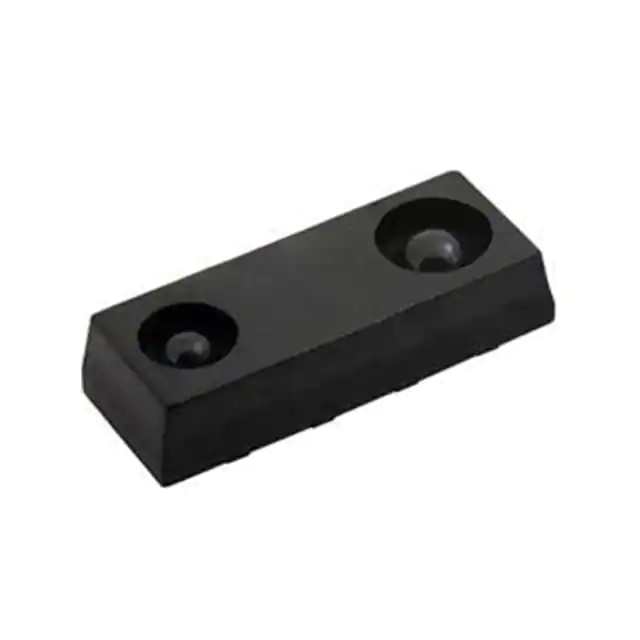
• Package type: surface-mount
• Dimensions (L x W x H in mm): 8.0 x 3.0 x 1.8
• Integrated modules: infrared emitter (IRED),
ambient light sensor (ALS), proximity sensor
(PS), and signal conditioning IC
• Operates ALS and PS in parallel structure
• FiltronTM technology adoption
background light cancellation
for
robust
• Supports low transmittance (dark) lens design
• Temperature compensation: -40 °C to +85 °C
DESCRIPTION
VCNL4100 integrates a high sensitivity long distance
proximity sensor (PS), ambient light sensor (ALS), and
940 nm IRED into one small package. It incorporates
photodiodes, amplifiers, and analog to digital converting
circuits into a single chip using a CMOS process. The 16-bit
high resolution ALS offers excellent sensing capabilities
with sufficient selections to fulfill most applications whether
a dark or high transparency lens design. VCNL4100 offers
individual programmable high and low threshold interrupt
features for the best utilization of resources and power
saving on the microcontroller. For the 8-bit proximity
sensing function, VCNL4100 has a built-in intelligent
cancellation scheme that eliminates background light
issues. The persistence feature prevents false judgment of
proximity sensing due to ambient light noise.
The adoption of the patented FiltronTM technology achieves
the closest ambient light spectral sensitivity to real human
eye responses. VCNL4100 provides excellent temperature
compensation capability for keeping the output stable under
changing temperature. ALS and PS functions are easily
operated via the simple command format of I2C (SMBus
compatible) interface protocol. Operating voltage ranges
from 2.5 V to 3.6 V.
4
• Floor life: 168 h, MSL 3, according to J-STD-020
• Output type: I2C bus (ALS / PS)
• Operation voltage: 2.5 V to 3.6 V
• Material categorization: for definitions of compliance
please see www.vishay.com/doc?99912
PROXIMITY FUNCTION
• Immunity to red glow (940 nm IRED)
• Intelligent background light cancellation
• Smart persistence scheme to reduce PS response time
• Proximity distance up to 1 m
AMBIENT LIGHT FUNCTION
• Fluorescent light flicker immunity
• Spectrum close to real human eye responses
• Selectable maximum detection range (655 / 1311 / 2621 /
5243) lux with highest sensitivity 0.01 lux/step
INTERRUPT
• Programmable interrupt function for ALS and PS with
upper and lower thresholds
PIN DEFINITION
5
• Low power consumption I2C (SMBus compatible)
interface
2
3
1
• Adjustable persistence to prevent false triggers for ALS
and PS
APPLICATIONS
6
7
9
8
10
• Collision detection in robots and toys
Top View
• Proximity sensing and lighting control in offices, corridors
and public buildings
1
GND
6
LED+
2
LED_Cathode
7
NC
3
VDD
8
INT
4
NC
9
SDAT
5
LED-
10
SCLK
Rev. 1.4, 24-Oct-17
• Presence detection to activate displays in printers,
copiers, and home appliances
• Vehicle occupancy detection in parking lots
• Proximity detection in lavatory appliances
Document Number: 84319
1
For technical questions, contact: sensorstechsupport@vishay.com
THIS DOCUMENT IS SUBJECT TO CHANGE WITHOUT NOTICE. THE PRODUCTS DESCRIBED HEREIN AND THIS DOCUMENT
ARE SUBJECT TO SPECIFIC DISCLAIMERS, SET FORTH AT www.vishay.com/doc?91000
�Not for New Designs
VCNL4100
www.vishay.com
Vishay Semiconductors
PRODUCT SUMMARY
PART
NUMBER
OPERATING
RANGE
(mm)
VCNL4100
0 to 1000
OPERATING I2C BUS
IRED PULSE
VOLTAGE VOLTAGE
CURRENT
RANGE
RANGE
(mA)
(V)
(V)
2.5 to 3.6
1.8 to 3.6
AMBIENT
LIGHT
RANGE
(lx)
800 (1)
AMBIENT
ADC RESOLUTION
LIGHT
OUTPUT
PROXIMITY /
RESOLUTION
CODE
AMBIENT LIGHT
(lx)
0.01 to 5243
0.01
16 bit, I2C
8 bit / 16 bit
Note
(1) Maximum allowed current for VCNL4100 internal IRED
ORDERING INFORMATION
ORDERING CODE
PACKAGING
VOLUME (1)
PIN NUMBER
REMARKS
VCNL4100
Tape and reel
MOQ: 2500 pcs
10
8.0 mm x 3.0 mm x 1.8 mm
Note
MOQ: minimum order quantity
(1)
ABSOLUTE MAXIMUM RATINGS (Tamb = 25 °C, unless otherwise specified)
PARAMETER
SYMBOL
MIN.
MAX.
Supply voltage
TEST CONDITION
VDD
-
5.0
UNIT
V
Operation temperature range
Tamb
-40
+85
°C
Storage temperature range
Tstg
-40
+100
°C
RECOMMENDED OPERATING CONDITIONS (Tamb = 25 °C, unless otherwise specified)
PARAMETER
TEST CONDITION
SYMBOL
MIN.
MAX.
UNIT
VDD
2.5
3.6
V
Operation temperature range
Tamb
-40
+85
°C
I2C bus operating frequency
f(I2CCLK)
10
400
kHz
Supply voltage
PIN DESCRIPTIONS
PIN ASSIGNMENT
SYMBOL
TYPE
1
GND
I
FUNCTION
Ground
2
LED_CATHODE
I
IRED cathode connection
3
VDD
I
Power supply input
4
NC
-
No connection
5
LED-
O
IRED cathode
6
LED+
I
IRED anode
7
NC
-
No connection
8
INT
O
Interrupt pin
9
SDAT
I / O (open drain)
I2C data bus data input / output
10
SCLK
I
I2C digital bus clock input
Rev. 1.4, 24-Oct-17
Document Number: 84319
2
For technical questions, contact: sensorstechsupport@vishay.com
THIS DOCUMENT IS SUBJECT TO CHANGE WITHOUT NOTICE. THE PRODUCTS DESCRIBED HEREIN AND THIS DOCUMENT
ARE SUBJECT TO SPECIFIC DISCLAIMERS, SET FORTH AT www.vishay.com/doc?91000
�Not for New Designs
VCNL4100
www.vishay.com
Vishay Semiconductors
BLOCK DIAGRAM
VDD
PS timing
controller
LED+
PS
buffer
DSP
IRED
LED-
PS
PD
Oscillator
INT
SCLK
SDAT
LED driver
LED_CATHODE
Temperature
sensor
I2C bus logic
control
ALS
PD
ALS
16-bits
data
buffer
Low pass filter
GND
BASIC CHARACTERISTICS (Tamb = 25 °C, unless otherwise specified)
PARAMETER
TEST CONDITION
SYMBOL
MIN.
TYP.
MAX.
UNIT
VDD
2.5
-
3.6
V
VIRED
3.8
-
5.0
V
Excluded LED driving
IDD
-
195
-
μA
Light condition = dark, VDD = 3.3 V
IDD (SD)
-
0.2
-
μA
ALS disable, PS enable
IALSSD
-
180
-
μA
ALS enable, PS disable
IPSSD
-
175
-
μA
VIH
1.5
-
-
VIL
-
-
0.8
VIH
1.4
-
-
VIL
-
-
0.6
Peak sensitivity wavelength of ALS
λp
-
550
-
Peak sensitivity wavelength of PS
λpps
-
940
-
nm
16-bit resolution
-
-
65 535
steps
steps
Supply voltage
Supply voltage for IRED
Supply current
Shutdown current
ALS shut down
PS shut down
Logic high
I2C signal input
Logic low
Logic high
Logic low
Full ALS counts
Full PS counts
VDD = 3.3 V
VDD = 2.6 V
V
nm
8-bit resolution
-
-
255
Minimum
IT = 640 ms, VDD = 3.3 V,
1 step (1)(2)
-
0.01
-
Maximum
IT = 80 ms, VDD = 3.3 V,
65 535 steps (1)(2)
-
5243
-
IT = 80 ms, VDD = 3.3 V,
normal sensitivity (1)
0
-
3
-40
-
+85
°C
-
-
800
mA
Detectable intensity
ALS dark offset
Operating temperature range
IRED driving current
V
lx
Tamb
(3)
steps
Notes
(1) Light source: white LED
(2) Maximum detection range to ambient light can be determined by ALS refresh time adjustment. Refer to table 17 “ALS Resolution and
Maximum Detection Range”
(3) Based on IRED on / off duty ratio = 1/5120, 1/640, 1/80, and 1/20. The circuitry should use an external MOSFET as shown with fig.10. Please
see also the Application Note “Designing the VCNL4100 into an Application” (www.vishay.com/doc?84361).
Rev. 1.4, 24-Oct-17
Document Number: 84319
3
For technical questions, contact: sensorstechsupport@vishay.com
THIS DOCUMENT IS SUBJECT TO CHANGE WITHOUT NOTICE. THE PRODUCTS DESCRIBED HEREIN AND THIS DOCUMENT
ARE SUBJECT TO SPECIFIC DISCLAIMERS, SET FORTH AT www.vishay.com/doc?91000
�Not for New Designs
VCNL4100
www.vishay.com
Vishay Semiconductors
I2C BUS TIMING CHARACTERISTICS (Tamb = 25 °C, unless otherwise specified)
PARAMETER
SYMBOL
Clock frequency
STANDARD MODE
MIN.
MAX.
f(SMBCLK)
10
t(BUF)
4.7
t(HDSTA)
Repeated start condition setup time
Stop condition setup time
Data hold time
t(HDDAT)
Data setup time
Bus free time between start and stop condition
Hold time after (repeated) start condition;
after this period, the first clock is generated
FAST MODE
UNIT
MIN.
MAX.
100
10
400
kHz
-
1.3
-
μs
4.0
-
0.6
-
μs
t(SUSTA)
4.7
-
0.6
-
μs
t(SUSTO)
4.0
-
0.6
-
μs
3450
-
900
ns
t(SUDAT)
250
-
100
-
ns
I2C clock (SCK) low period
t(LOW)
4.7
-
1.3
-
μs
I2C clock (SCK) high period
t(HIGH)
4.0
-
0.6
-
μs
t(TIMEOUT)
25
35
-
-
ms
Clock / data fall time
t(F)
-
300
-
300
ns
Clock / data rise time
t(R)
-
1000
-
300
ns
Detect clock / data low timeout
t(LOW)
I2C bus
CLOCK
(SCLK)
t(R)
t(F)
V IH
V IL
t(HDSTA)
t(SUSTA )
t(HIGH)
t(SUSTO)
t(BUF)
t(HDDAT)
I2C bus
DATA
(SDAT)
t(SUDAT)
V IH
V IL
{
P
Stop Condition
{
{
S
Start Condition
{
S
Start
P
Stop
t(LOSEXT )
SCLKACK
t(LOWMEXT )
SDA ACK
t(LOWMEXT )
t(LOWMEXT )
2
I C bus
CLOCK
(SCLK)
I2C bus
DATA
(SDAT)
Fig. 1 - I2C Bus Timing Diagram
Rev. 1.4, 24-Oct-17
Document Number: 84319
4
For technical questions, contact: sensorstechsupport@vishay.com
THIS DOCUMENT IS SUBJECT TO CHANGE WITHOUT NOTICE. THE PRODUCTS DESCRIBED HEREIN AND THIS DOCUMENT
ARE SUBJECT TO SPECIFIC DISCLAIMERS, SET FORTH AT www.vishay.com/doc?91000
�Not for New Designs
VCNL4100
www.vishay.com
Vishay Semiconductors
PARAMETER TIMING INFORMATION
I2C BUS
CLOCK
(SCLK)
I2C BUS
DATA
(SDAT)
SA7
SA6
SA5
SA4
SA3
W
SA1
SA2
Start by
Master
SA7
SA6
SA5
SA4
SA3
SA1
SA2
SA0
ACK by
VCNL4100
ACK by
VCNL4100
2
I C Bus Slave Address Byte
Command Code
I2C BUS
CLOCK
(SCLK)
I2C BUS
DATA
(SDAT)
SA7
SA6
SA5
SA4
SA3
SA2
SA0
SA1
SA7
SA6
SA5
SA4
SA3
SA2
SA1
SA0
ACK by
VCNL4100
ACK by
VCNL4100
Data Byte Low
Stop by
Master
Data Byte High
Fig. 2 - I2C Bus Timing for Sending Word Command Format
I2C BUS
CLOCK
(SCLK)
I2C BUS
DATA
(SDAT)
SA7
SA6
SA5
SA4
SA3
W
SA1
SA2
Start by
Master
SA7
SA6
SA5
SA4
SA3
SA0
SA1
SA2
ACK by
VCNL4100
ACK by
VCNL4100
2
Command Code
I C Bus Slave Address Byte
I2C BUS
CLOCK
(SCLK)
I2C BUS
DATA
(SDAT)
SA6
SA7
SA5
SA4
SA3
SA2
R
SA1
Start by
Master
SA7
SA6
SA5
SA4
SA3
SA2
SA1
SA0
ACK by
Master
ACK by
VCNL4100
2
Data Byte Low
I C Bus Slave Address Byte
I2C BUS
CLOCK
(SCLK)
I2C BUS
DATA
(SDAT)
SA7
SA6
SA5
SA4
SA3
SA2
SA1
SA0
NACK by
Master
Stop by
Master
Data Byte High
Fig. 3 - I2C Bus Timing for Receiving Word Command Format
Rev. 1.4, 24-Oct-17
Document Number: 84319
5
For technical questions, contact: sensorstechsupport@vishay.com
THIS DOCUMENT IS SUBJECT TO CHANGE WITHOUT NOTICE. THE PRODUCTS DESCRIBED HEREIN AND THIS DOCUMENT
ARE SUBJECT TO SPECIFIC DISCLAIMERS, SET FORTH AT www.vishay.com/doc?91000
�Not for New Designs
VCNL4100
www.vishay.com
Vishay Semiconductors
TYPICAL PERFORMANCE CHARACTERISTICS (Tamb = 25 °C, unless otherwise specified)
PS
ALS
Fig. 7 - IDD vs.Temperature
Fig. 4 - Normalized Spectral Response
Axis Title
1.1
10000
0.9
0.8
1000
0.7
1st line
2nd line
Relative Radiant Intensity
Normalized Output
1.0
0.6
0.5
0.4
100
0.3
0.2
0.1
10
0
-90
-60
0
-30
30
60
90
View Angle
2nd line
Fig. 5 - ALS Normalized Output vs. View Angle
Fig. 8 - Relative Radiant Intensity vs. Angular Displacement
Axis Title
Axis Title
70 000
1.0
10000
0.9
1000
1st line
2nd line
640 ms
40 000
320 ms
30 000
160 ms
100
20 000
80 ms
10 000
0.8
0.7
1000
0.6
1st line
2nd line
50 000
Relative Radiant Intensity
Relative Radiant Intensity
60 000
Step
Step
10000
0.5
0.4
100
0.3
0.2
0.1
0
0
2000
4000
6000
8000
10
10 000
0
-100 -75
10
-50
-25
0
25
50
75
100
Lux
2nd line
View Angle
2nd line
Fig. 6 - ALS Refresh Time vs. Maximum Detection Range
Fig. 9 - Relative Radiant Intensity vs. Angular Displacement
Rev. 1.4, 24-Oct-17
Document Number: 84319
6
For technical questions, contact: sensorstechsupport@vishay.com
THIS DOCUMENT IS SUBJECT TO CHANGE WITHOUT NOTICE. THE PRODUCTS DESCRIBED HEREIN AND THIS DOCUMENT
ARE SUBJECT TO SPECIFIC DISCLAIMERS, SET FORTH AT www.vishay.com/doc?91000
�Not for New Designs
VCNL4100
www.vishay.com
Vishay Semiconductors
APPLICATION INFORMATION
Pin Connection with the Host
VCNL4100 is a cost effective solution of a long distance proximity sensor with I2C interface. The standard serial digital interface
easily accesses “light intensity” by using simple calculations.
Application circuitry below shows the added MOSFET which is driven by the ASIC’s pin 2. A 22 kΩ pull-up resistor needs to be
added here. The RLED defines the current through the IRED. A small 0.1 μF is sufficient at VDD for power supply noise rejection,
but a 2.2 μF should be placed at VIRED to provide the energy for the IRED.
For the I2C bus design, the pull-up voltage refers to the I/O specification of the baseband due to its “open drain” design. The
pull-high resistors for the I2C bus lines are recommended to be ≥ 2.2 kΩ.
Vpull up
VDD
VIRED
0.1 μF
2.2 kΩ
2.2 kΩ
2.2 μF
20 kΩ
3
VDD
10
SCLK
SCLK
SCK
9
SDA
MCU
S
LED 2
CATHODE
PMOS
G
D
SDAT
VCNL4100
8.2 kΩ
LED+ 6
8
INT
LED- 5
INT
INT
RLED
2.7 Ω
GND
1
Fig. 10 - Application Diagram
Notes
• VDD range: 2.5 V to 3.6 V and VIRED is recommended 5.0 V
• Power path of VDD and VIRED should be routed separately up to stable power source.
• The RLED resister value should be evaluated within ready-made application and the current through VCNL4100-internal IRED should not
exceed 800 mA.
Digital Interface
VCNL4100 applies single 7-bit slave address 0x60 (HEX) following I2C protocol. All operations can be controlled by the
command register. The simple command structure helps users easily program the operation setting and latch the light data from
VCNL4100. As fig. 11 shows, VCNL4100’s I2C command format is simple for read and write operations between VCNL4100
and the host. The white sections indicate host activity and the gray sections indicate VCNL4100’s acknowledgement of the host
access activity. Write word and read word protocols are suitable for accessing registers particularly for 16-bit ALS data and
8-bit PS data. Interrupt can be cleared by reading data out from register: INT_Flag.
Send Byte ɦ Write Command to VCNL4100
1
S
1
1
8
1
8
1
8
1
1
Wr
A
Command Code
A
Data Byte Low
A
Data Byte High
A
P
7
Slave Address
Receive Byte ɦ Read Data from VCNL4100
1
7
1
1
8
1
1
7
1
1
8
1
8
1
1
S
Slave Address
Wr
A
Command Code
A
S
Slave Address
Rd
A
Data Byte Low
A
Data Byte High
N
P
S = start condition
P = stop condition
A = acknowledge
Shaded area = VCNL4100 acknowledge
Fig. 11 - Command Protocol Format
Rev. 1.4, 24-Oct-17
Document Number: 84319
7
For technical questions, contact: sensorstechsupport@vishay.com
THIS DOCUMENT IS SUBJECT TO CHANGE WITHOUT NOTICE. THE PRODUCTS DESCRIBED HEREIN AND THIS DOCUMENT
ARE SUBJECT TO SPECIFIC DISCLAIMERS, SET FORTH AT www.vishay.com/doc?91000
�Not for New Designs
VCNL4100
www.vishay.com
Vishay Semiconductors
Function Description
VCNL4100 applies a 16-bit high resolution ALS that provides the best ambient light sensing capability up to 0.011375 lx/step
which works well under a low transmittance lens design (dark lens). A flexible interrupt function of ALS (register: ALS_CONF) is
also supported. The INT signal will not be asserted by VCNL4100 if the ALS value is not over high INT threshold window level,
or lower than low INT threshold window level of ALS. As long as the ALS INT is asserted, the host can read the data from
VCNL4100.
For proximity sensor function, VCNL4100 supports different kinds of mechanical design to achieve the best proximity detection
performance for any color object. The basic PS function settings, such as duty ratio, integration time, interrupt, and PS
enable / disable and persistence, are handled by the register: PS_CONF1. Duty ratio controls the PS response time. Integration
time represents the duration of the energy being received. The interrupt is asserted when the PS detection levels over the high
threshold level setting (register: PS_THDH) or lower than low threshold (register: PS_THDL). If the interrupt function is enabled,
the host reads the PS output data from VCNL4100 that saves host loading from periodically reading PS data. More than that,
INT flag (register: INT_Flag) indicates the behavior of INT triggered under different conditions. PS persistence (PS_PERS) sets
up the PS INT asserted conditions as long as the PS output value continually exceeds the threshold level.
Descriptions of each slave address operation are shown in table 1.
TABLE 1 - COMMAND CODE AND REGISTER DESCRIPTION
COMMAND
CODE
00H_L
REGISTER
NAME
ALS_CONF
R/W
DEFAULT
VALUE
R/W
00H
FUNCTION DESCRIPTION
ALS integration time, persistence, interrupt, and function enable / disable
00H_H
Reserved
R/W
00H
Reserved
01H_L
ALS_THDH_L
R/W
00H
ALS high interrupt threshold LSB byte
01H_H
ALS_THDH_M
R/W
00H
ALS high interrupt threshold MSB byte
02H_L
ALS_THDL_L
R/W
00H
ALS low interrupt threshold LSB byte
02H_H
ALS_THDL_M
R/W
00H
ALS low interrupt threshold MSB byte
03H_L
PS_CONF1
R/W
00H
PS duty ratio, integration time, persistence, and PS enable / disable
03H_H
PS_CONF2
R/W
00H
PS gain, ITB, interrupt setting
04H_L
PS_CONF3
R/W
00H
PS active forced, averaging, background light cancellation setting
04H_H
PS_SPO
R/W
00H
Set initial value to “0xA0” or “0x20”
05H_L
Reserved
R/W
00H
Reserved
05H_H
Reserved
R/W
00H
Reserved
06H_L
PS_THDL
R/W
00H
PS low interrupt threshold setting
06H_H
PS_THDH
R/W
00H
PS high interrupt threshold setting
07H_L
Reserved
R/W
00H
Reserved
07H_H
Reserved
R/W
00H
Reserved
08H_L
PS_Data
R
00H
PS output data
08H_H
Reserved
R
00H
Reserved
09H_L
ALS_Data_L
R
00H
ALS LSB output data
09H_H
ALS_Data_M
R
00H
ALS MSB output data
0AH_L
Reserved
R
00H
Reserved
0AH_H
Reserved
R
00H
Reserved
0BH_L
Reserved
R
00H
Reserved
0BH_H
INT_Flag
R
00H
ALS, PS interrupt flags
Rev. 1.4, 24-Oct-17
Document Number: 84319
8
For technical questions, contact: sensorstechsupport@vishay.com
THIS DOCUMENT IS SUBJECT TO CHANGE WITHOUT NOTICE. THE PRODUCTS DESCRIBED HEREIN AND THIS DOCUMENT
ARE SUBJECT TO SPECIFIC DISCLAIMERS, SET FORTH AT www.vishay.com/doc?91000
�Not for New Designs
VCNL4100
www.vishay.com
Vishay Semiconductors
Command Register Format
VCNL4100 provides an 8-bit command register for ALS and PS controlling independently. The description of each command
format is shown in following tables.
TABLE 2 - REGISTER: ALS_CONF DESCRIPTION
REGISTER NAME
Command
COMMAND CODE: 0xH_L (0xH DATA BYTE LOW) OR 0xH_H (0xH DATA BYTE HIGH)
Bit
7
6
ALS_CONF
Command
5
4
3
2
1
0
COMMAND CODE: 00H_L (00H DATA BYTE LOW)
Bit
Description
ALS_IT
7:6
(0 : 0) = 80 ms; (0 : 1) = 160 ms; (1 : 0) = 320 ms; (1 : 1) = 640 ms
ALS integration time setting, longer integration time has higher sensitivity
Reserved
5:4
Default = (0 : 0), reserved
ALS_PERS
3:2
(0 : 0) = 1, (0 : 1) = 2, (1 : 0) = 4, (1 : 1) = 8
ALS interrupt persistence setting
ALS_INT_EN
1
0 = ALS interrupt disable, 1 = ALS interrupt enable
ALS_SD
0
0 = ALS power on, 1 = ALS shut down
TABLE 3 - REGISTER: RESERVE COMMAND DESCRIPTION
Reserved
COMMAND CODE: 00H_H (00H DATA BYTE HIGH)
Command
Bit
Reserved
7:0
Description
Default = 00H
TABLE 4 - REGISTER ALS_THDH_L AND ALS_THDH_M DESCRIPTION
ALS_THDH_L
ALS_THDH_M
Register
COMMAND CODE: 01H_L (01H DATA BYTE LOW)
COMMAND CODE: 01H_H (01H DATA BYTE HIGH)
Bit
Description
ALS_THDH_L
7:0
00H to FFH, ALS high interrupt threshold LSB byte
ALS_THDH_M
7:0
00H to FFH, ALS high interrupt threshold MSB byte
TABLE 5 - REGISTER: ALS_THDL_L AND ALS_THDL_M DESCRIPTION
ALS_THDL_L
ALS_THDL_M
Register
COMMAND CODE: 02H_L (02H DATA BYTE LOW)
COMMAND CODE: 02H_H (02H DATA BYTE HIGH)
Bit
Description
ALS_THDL_L
7:0
00H to FFH, ALS low interrupt threshold LSB byte
ALS_THDL_M
7:0
00H to FFH, ALS low interrupt threshold MSB byte
TABLE 6 - REGISTER: PS_CONF1 DESCRIPTION
PS_CONF1
Command
COMMAND CODE: 03H_L (03H DATA BYTE LOW)
Bit
Description
PS_Duty
7:6
(0 : 0) = 1/5120, (0 : 1) = 1/640, (1 : 0) = 1/80, (1 : 1) = 1/20
PS IRED on / off duty ratio setting
PS_ IT
5:4
(0 : 0) = 1T, (0 : 1) = 1.3T, (1 : 0) = 1.6T, (1 : 1) = 2T
PS integration time setting
PS_PERS
3:2
(0 : 0) = 1, (0 : 1) = 2, (1 : 0) = 3, (1 : 1) = 4
PS interrupt persistence setting
Reserved
1
Default = 0, reserved
PS_SD
0
0 = PS power on, 1 = PS shut down
Rev. 1.4, 24-Oct-17
Document Number: 84319
9
For technical questions, contact: sensorstechsupport@vishay.com
THIS DOCUMENT IS SUBJECT TO CHANGE WITHOUT NOTICE. THE PRODUCTS DESCRIBED HEREIN AND THIS DOCUMENT
ARE SUBJECT TO SPECIFIC DISCLAIMERS, SET FORTH AT www.vishay.com/doc?91000
�Not for New Designs
VCNL4100
www.vishay.com
Vishay Semiconductors
TABLE 7 - REGISTER: PS_CONF2 DESCRIPTION
PS_CONF2
Command
COMMAND CODE: 03H_H (03H DATA BYTE HIGH)
Bit
Description
(0 : 0) = 1/2T, (0 : 1) = 1T, (1 : 0) = 2T, (1 : 1) = 4T
PS IT bank setting
PS_ITB
7:6
PS_GAIN
5:4
Reserved
3
Default = 0, reserved
PS_SP_INT_EN
2
0 = disable INT function for PS enter / leave sunlight protection mode
1 = issue INT while PS enter / leave sunlight protection mode. While PS enter sunlight protection mode,
the PS output will keep 0xFF
Reserved
1
Default = 0, reserved
0
0 = PS INT function disable
1 = PS INT function enable
PS_INT_EN
(0 : 0) = /4, (0 : 1) = /2, (1 : 0) = 1, (1 : 1) = 2
TABLE 8 - REGISTER: PS_CONF3 DESCRIPTION
PS_CONF3
Command
PS_AV
COMMAND CODE: 04H_L (04H DATA BYTE LOW)
Bit
7:6
Description
(0 : 0) = /2, (0 : 1) = /4, (1 : 0) = /8, (1 : 1) = /16
PS_AV_EN
5
0 = PS average function disable, 1 = PS average function enable
Reserved
4
Default = 0, reserved
PS_AF
3
0 = active force mode disable (normal mode), 1 = active force mode enable
PS_TRIG
2
0 = no PS active force mode trigger, 1 = trigger one time cycle
VCNL4100 output one cycle data every time host writes in “1” to sensor. The state returns to “0”
automatically.
PS_MPULSE
1
0 = disable, 1 = enable
PS multi pulse mode setting; PS multi pulse number set by PS_AV [1 : 0]
Reserved
0
Default = 0, reserved
TABLE 9 - REGISTER: PS_MS DESCRIPTION
Reserved
Command
PS_SPO
COMMAND CODE: 04H_H (04H DATA BYTE HIGH)
Bit
7:0
Description
Set initial value = 0xA0 (PS_OUT = 0xFF while PS into sunlight protection
Set initial value = 0x20 (PS_OUT = 0x00 while PS into sunlight protection
TABLE 10 - REGISTER RESERVE COMMAND DESCRIPTION
Reserved
COMMAND CODE: 05H_L (05H DATA BYTE LOW)
Register
Bit
Reserved
7:0
Description
Default = 00H
TABLE 11 - REGISTER: RESERVE COMMAND DESCRIPTION
Reserved
COMMAND CODE: 05H_H (05H DATA BYTE HIGH)
Register
Bit
Reserved
7:0
Description
Default = 00H
TABLE 12 - REGISTER: PS_THDL DESCRIPTION
PS_THDL
Register
PS_THDL
Rev. 1.4, 24-Oct-17
COMMAND CODE: 06H_L (06H DATA BYTE LOW)
Bit
7:0
Description
00H to FFH, PS low interrupt threshold setting
Document Number: 84319
10
For technical questions, contact: sensorstechsupport@vishay.com
THIS DOCUMENT IS SUBJECT TO CHANGE WITHOUT NOTICE. THE PRODUCTS DESCRIBED HEREIN AND THIS DOCUMENT
ARE SUBJECT TO SPECIFIC DISCLAIMERS, SET FORTH AT www.vishay.com/doc?91000
�Not for New Designs
VCNL4100
www.vishay.com
Vishay Semiconductors
TABLE 13 - REGISTER: PS_THDH DESCRIPTION
PS_THDH
Register
PS_THDH
COMMAND CODE: 06H_H (06H DATA BYTE HIGH)
Bit
7:0
Description
00H to FFH, PS high interrupt threshold setting
TABLE 14 - REGISTER: RESERVE COMMAND DESCRIPTION
Reserved
COMMAND CODE: 07H_L (07H DATA BYTE LOW)
Register
Bit
Reserved
7:0
Description
Default = 00H
TABLE 15 - REGISTER: RESERVE COMMAND DESCRIPTION
Reserved
COMMAND CODE: 07H_H (07H DATA BYTE HIGH)
Register
Bit
Reserved
7:0
Description
Default = 00H
TABLE 16 - READ OUT REGISTER DESCRIPTION
REGISTER
COMMAND CODE
BIT
08H_L (08H data byte low)
Reserved
08H_H (08H data byte high)
7:0
Default = 00H
ALS_Data_L
09H_L (09H data byte low)
7:0
00H to FFH, ALS LSB output data
ALS_Data_M
09H_H (09H data byte high)
7:0
00H to FFH, ALS MSB output data
Reserved
0AH_L (0AH data byte low)
7:0
Reserved
0AH_H (0AH data byte high)
7:0
Reserved
0BH_L (0BH data byte low)
7:0
0BH_H (0BH data byte high)
7
6
5
4
3
2
1
0
INT_Flag
7:0
DESCRIPTION
PS_Data
00H to FFH, PS output data
Default = 00H
PS_SPF_LEAVE, PS leaving protection mode
PS_SPF_ENTER, PS entering protection mode
ALS_IF_L, ALS crossing low THD INT trigger event
ALS_IF_H, ALS crossing high THD INT trigger event
Default = 0, reserved
Default = 0, reserved
PS_IF_CLOSE, PS rise above PS_THDH INT trigger event
PS_IF_AWAY, PS drop below PS_THDL INT trigger event
Adjustable Sampling Time
VCNL4100’s embedded LED driver drives the external IRED with the “LED CATHODE” pin by a pulsed duty cycle. The
IRED on / off duty ratio can be programmable by I2C command at register: PS_Duty is related to the current consumption and
PS response time. The higher the duty ratio selected, the faster response time achieved with higher power consumption.
Rev. 1.4, 24-Oct-17
Document Number: 84319
11
For technical questions, contact: sensorstechsupport@vishay.com
THIS DOCUMENT IS SUBJECT TO CHANGE WITHOUT NOTICE. THE PRODUCTS DESCRIBED HEREIN AND THIS DOCUMENT
ARE SUBJECT TO SPECIFIC DISCLAIMERS, SET FORTH AT www.vishay.com/doc?91000
�Not for New Designs
VCNL4100
www.vishay.com
Vishay Semiconductors
Threshold Window Setting
• ALS Threshold Window Setting (Applying ALS INT)
Register: ALS_THDH_L and ALS_THDH_M define 16-bit ALS high threshold data for LSB byte and MSB byte. Register:
ALS_THDL_L and ALS_THDL_M define 16-bit ALS low threshold data for LSB byte and MSB byte. As long as ALS INT
function is enabled, INT will be asserted once the ALS data exceeds ALS_THDH or goes below ALS_THDL. To easily define
the threshold range, multiply the value of the resolution (lx/step) by the threshold level (refer table 17).
TABLE 17 - ALS RESOLUTION AND MAXIMUM DETECTION RANGE
ALS_IT
ALS_IT
(7 : 6)
MAXIMUM DETECTION
RANGE
(lx)
SENSITIVITY
(lx/step)
INTEGRATION TIME
(0, 0)
80 ms
0.08
5243
(0, 1)
160 ms
0.04
2621
(1, 0)
320 ms
0.02
1311
(1, 1)
640 ms
0.01
655
The following is an example of the application for ALS_IT = 160 ms. If ALS_THDH = 07D0(HEX) and ALS_THDL = 03E8(HEX),
then the ALS INT will not asserted if the ALS value does not exceed 80 lx [07D0(HEX) = 2000 steps x 0.04 lx/step = 80 lx] or
lower than 40 lx [03E8(HEX) = 1000 steps x 0.04 lx/step = 40 lx.
• ALS Persistence
The ALS INT is asserted as long as the ALS value is higher or lower than the threshold window when ALS_PERS
(1 / 2 / 4 / 8 times) is set to one time. If ALS_PERS is set to four times, then the ALS INT will not be asserted if the
ALS value is not over (or lower) than the threshold window for four continued refresh times (integration time).
• Programmable PS Threshold
VCNL4100 provides both high and low thresholds 8-bit data setting for proximity sensor. (register: PS_THDL, PS_THDH) that
fulfills different mechanical designs with the best proximity detection capability for any kind of objects.
• PS Persistence
The PS persistence function (PS_PERS 1 / 2 / 3 / 4) helps to avoid false trigger of the PS INT. For example, if
PS_PERS = 3 times, the PS INT will not be asserted unless the PS value is greater than the PS threshold (PS1_THDH)
value for three periods of time continuously.
Data Access
All VCNL4100 command registers are readable. To access 16-bit high resolution ALS output data, it is suitable to use read word
protocol to read out data by just one command at register: ALS_Data_L and ALS_Data_M. To represent the 16-bit data of ALS,
it has to apply two bytes. One byte is for LSB, and the other byte is for MSB as shown in table 18. In terms of reading out 8-bit
PS data, host just need to access register: PS_Data.
TABLE 18 - 16-BIT ALS DATA FORMAT
VCNL4100
Bit
15
Register
14
13
12
11
ALS_Data_M
10
9
8
7
6
5
4
3
2
1
0
ALS_Data_L
Interrupt (INT)
VCNL4100 has ALS and PS interrupt feature operated by a single pin “INT”. The purpose of the interrupt feature is to actively
inform the host once INT has been asserted. With the interrupt function applied, the host does not need to constantly pull data
from the sensor, but to only read data from the sensor when receiving interrupt request from the sensor. As long as the host
enables ALS interrupt (register: ALS_INT_EN) or PS interrupt (register: PS_INT) function, the level of INT pin (pin 8) is able to be
pulled low once INT asserted. All of registers are accessible even INT is asserted.
ALS INT asserted when ALS value crosses over the value set by register: ALS_THDH or is lower than the value set by
register: ALS_THDL.
PS INT asserted when PS value crosses over the value set by register: PS_THDH or is lower than the value set by
register: PS_THDL.
Rev. 1.4, 24-Oct-17
Document Number: 84319
12
For technical questions, contact: sensorstechsupport@vishay.com
THIS DOCUMENT IS SUBJECT TO CHANGE WITHOUT NOTICE. THE PRODUCTS DESCRIBED HEREIN AND THIS DOCUMENT
ARE SUBJECT TO SPECIFIC DISCLAIMERS, SET FORTH AT www.vishay.com/doc?91000
�Not for New Designs
VCNL4100
www.vishay.com
Vishay Semiconductors
Interrupt Flag
Register: INT_Flag represents all of interrupt trigger status for ALS and PS. Any flag value changes from “0” to “1” state, the
level of INT pin will be pulled low. As long as host reads INT_Flag data, the bit will change from “1” state to “0” state after reading
out. The INT level will be returned to high afterwards.
PROXIMITY DETECTION HYSTERESIS
A PS detection hysteresis is important to keep the PS state in a certain range of detection distance. For example, PS INT asserts
when PS value over PS_THDH. Host switches on panel backlight and then clears INT. When PS value is less than PS_THDL,
host switches off panel backlight. Any PS value lower than PS_THDH or higher than PS_THDL PS INT will not be asserted. Host
keeps the same state.
PACKAGE INFORMATION in millimeters
Side View
3.0 ± 0.1
1.8 ± 0.1
5
1.0
5
6
1.7
6
Bottom View
5
7
4
8
3
9
2
10
1
1.7
Ø 1.7
6
5.0
8.0 ± 0.1
LED
1.0 (10 x)
Top View
Ø 2.05
1.6
.6
Sensor
1
10
10
1.2
1
0.8
1.2
2.0
0.8
1.2
For Reflow Soldering (PCB Footprint)
1
GND
6
LED+
2
LED_Cathode
7
NC
3
VDD
8
INT
4
NC
9
SDAT
5
LED-
10
SCLK
1.7
Fig. 12 - VCNL4100 Package Dimensions
Rev. 1.4, 24-Oct-17
Document Number: 84319
13
For technical questions, contact: sensorstechsupport@vishay.com
THIS DOCUMENT IS SUBJECT TO CHANGE WITHOUT NOTICE. THE PRODUCTS DESCRIBED HEREIN AND THIS DOCUMENT
ARE SUBJECT TO SPECIFIC DISCLAIMERS, SET FORTH AT www.vishay.com/doc?91000
�Not for New Designs
VCNL4100
www.vishay.com
Vishay Semiconductors
LAYOUT NOTICE AND REFERENCE CIRCUIT
Circuit Layout Reference
Fig. 13 - Suggested VCNL4100 Layout
APPLICATION CIRCUIT BLOCK REFERENCE
Vpull up
VDD
VIRED
0.1 μF
2.2 kΩ
2.2 kΩ
2.2 μF
20 kΩ
3
VDD
10
SCLK
SCLK
SCK
9
SDA
MCU
S
LED 2
CATHODE
PMOS
G
D
SDAT
VCNL4100
8.2 kΩ
LED+ 6
8
INT
LED- 5
INT
INT
RLED
GND
2.7 Ω
1
Fig. 14 - VCNL4100 Application Circuit
Notes
• VDD range: 2.5 V to 3.6 V and VIRED is recommended 5.0 V
• Power path of VDD and VIRED should be independent layout
• The RLED resistor value is reference for test stage, it should be adjusted again for the product usage basing on the power and the lens final
design.
RECOMMENDED STORAGE AND REBAKING CONDITIONS
PARAMETER
MIN.
MAX.
UNIT
Storage temperature
5
50
°C
Relative humidity
-
60
%
Open time
-
168
h
From the date code on the aluminized envelope (unopened)
-
12
months
Tape and reel: 60 °C
-
22
h
Tube: 60 °C
-
22
h
Total time
Rebaking
Rev. 1.4, 24-Oct-17
CONDITIONS
Document Number: 84319
14
For technical questions, contact: sensorstechsupport@vishay.com
THIS DOCUMENT IS SUBJECT TO CHANGE WITHOUT NOTICE. THE PRODUCTS DESCRIBED HEREIN AND THIS DOCUMENT
ARE SUBJECT TO SPECIFIC DISCLAIMERS, SET FORTH AT www.vishay.com/doc?91000
�Not for New Designs
VCNL4100
www.vishay.com
Vishay Semiconductors
RECOMMENDED INFRARED REFLOW
Soldering conditions which are based on J-STD-020 C.
IR REFLOW PROFILE CONDITION
PARAMETER
CONDITIONS
Peak temperature
TEMPERATURE
TIME
255 °C + 0 °C / - 5 °C (max.: 260 °C)
10 s
150 °C to 200 °C
60 s to 180 s
217 °C
60 s to 150 s
Preheat temperature range and timing
Timing within 5 °C to peak temperature
10 s to 30 s
Timing maintained above temperature / time
Timing from 25 °C to peak temperature
8 min (max.)
Ramp-up rate
3 °C/s (max.)
Ramp-down rate
6 °C/s (max.)
Temperature (°C)
Recommend Normal Solder Reflow is 235 °C to 255 °C.
Max. Temperature
(260 °C + 0 °C / - 5 °C)/10 s
255
Ramp-Up Rate
3 °C/s (max.)
217
Ramp-Down Rate
6 °C/s (max.)
200
150
Soldering Zone
60 s to 150 s
Ramp-Up Rate
3 °C/s (max.)
Pre-Heating Time
t2 - t1 = 60 s to 180 s
t2
t1
Time (s)
Fig. 15 - VCNL4100 Solder Reflow Profile Chart
RECOMMENDED IRON TIP SOLDERING CONDITION AND WARNING HANDLING
1. Solder the device with the following conditions:
1.1. Soldering temperature: 400 °C (max.)
1.2. Soldering time: 3 s (max.)
2. If the temperature of the method portion rises in addition to the residual stress between the leads, the possibility that an
open or short circuit occurs due to the deformation or destruction of the resin increases.
3. The following methods: VPS and wave soldering, have not been suggested for the component assembly.
4. Cleaning method conditions:
4.1. Solvent: methyl alcohol, ethyl alcohol, isopropyl alcohol
4.2. Solvent temperature < 45 °C (max.)
4.3. Time: 3 minutes (min.)
Rev. 1.4, 24-Oct-17
Document Number: 84319
15
For technical questions, contact: sensorstechsupport@vishay.com
THIS DOCUMENT IS SUBJECT TO CHANGE WITHOUT NOTICE. THE PRODUCTS DESCRIBED HEREIN AND THIS DOCUMENT
ARE SUBJECT TO SPECIFIC DISCLAIMERS, SET FORTH AT www.vishay.com/doc?91000
�Not for New Designs
VCNL4100
www.vishay.com
Vishay Semiconductors
TAPE PACKAGING INFORMATION in millimeters
Fig. 16 - Package Carrier Tape
Fig. 17 - Reel Dimensions
Rev. 1.4, 24-Oct-17
Document Number: 84319
16
For technical questions, contact: sensorstechsupport@vishay.com
THIS DOCUMENT IS SUBJECT TO CHANGE WITHOUT NOTICE. THE PRODUCTS DESCRIBED HEREIN AND THIS DOCUMENT
ARE SUBJECT TO SPECIFIC DISCLAIMERS, SET FORTH AT www.vishay.com/doc?91000
�Legal Disclaimer Notice
www.vishay.com
Vishay
Disclaimer
ALL PRODUCT, PRODUCT SPECIFICATIONS AND DATA ARE SUBJECT TO CHANGE WITHOUT NOTICE TO IMPROVE
RELIABILITY, FUNCTION OR DESIGN OR OTHERWISE.
Vishay Intertechnology, Inc., its affiliates, agents, and employees, and all persons acting on its or their behalf (collectively,
“Vishay”), disclaim any and all liability for any errors, inaccuracies or incompleteness contained in any datasheet or in any other
disclosure relating to any product.
Vishay makes no warranty, representation or guarantee regarding the suitability of the products for any particular purpose or
the continuing production of any product. To the maximum extent permitted by applicable law, Vishay disclaims (i) any and all
liability arising out of the application or use of any product, (ii) any and all liability, including without limitation special,
consequential or incidental damages, and (iii) any and all implied warranties, including warranties of fitness for particular
purpose, non-infringement and merchantability.
Statements regarding the suitability of products for certain types of applications are based on Vishay's knowledge of typical
requirements that are often placed on Vishay products in generic applications. Such statements are not binding statements
about the suitability of products for a particular application. It is the customer's responsibility to validate that a particular product
with the properties described in the product specification is suitable for use in a particular application. Parameters provided in
datasheets and / or specifications may vary in different applications and performance may vary over time. All operating
parameters, including typical parameters, must be validated for each customer application by the customer's technical experts.
Product specifications do not expand or otherwise modify Vishay's terms and conditions of purchase, including but not limited
to the warranty expressed therein.
Hyperlinks included in this datasheet may direct users to third-party websites. These links are provided as a convenience and
for informational purposes only. Inclusion of these hyperlinks does not constitute an endorsement or an approval by Vishay of
any of the products, services or opinions of the corporation, organization or individual associated with the third-party website.
Vishay disclaims any and all liability and bears no responsibility for the accuracy, legality or content of the third-party website
or for that of subsequent links.
Except as expressly indicated in writing, Vishay products are not designed for use in medical, life-saving, or life-sustaining
applications or for any other application in which the failure of the Vishay product could result in personal injury or death.
Customers using or selling Vishay products not expressly indicated for use in such applications do so at their own risk. Please
contact authorized Vishay personnel to obtain written terms and conditions regarding products designed for such applications.
No license, express or implied, by estoppel or otherwise, to any intellectual property rights is granted by this document or by
any conduct of Vishay. Product names and markings noted herein may be trademarks of their respective owners.
© 2022 VISHAY INTERTECHNOLOGY, INC. ALL RIGHTS RESERVED
Revision: 01-Jan-2022
1
Document Number: 91000
�


 工商网监
湘ICP备2023018690号
工商网监
湘ICP备2023018690号