VEMD8080
www.vishay.com
Vishay Semiconductors
Silicon PIN Photodiode
FEATURES
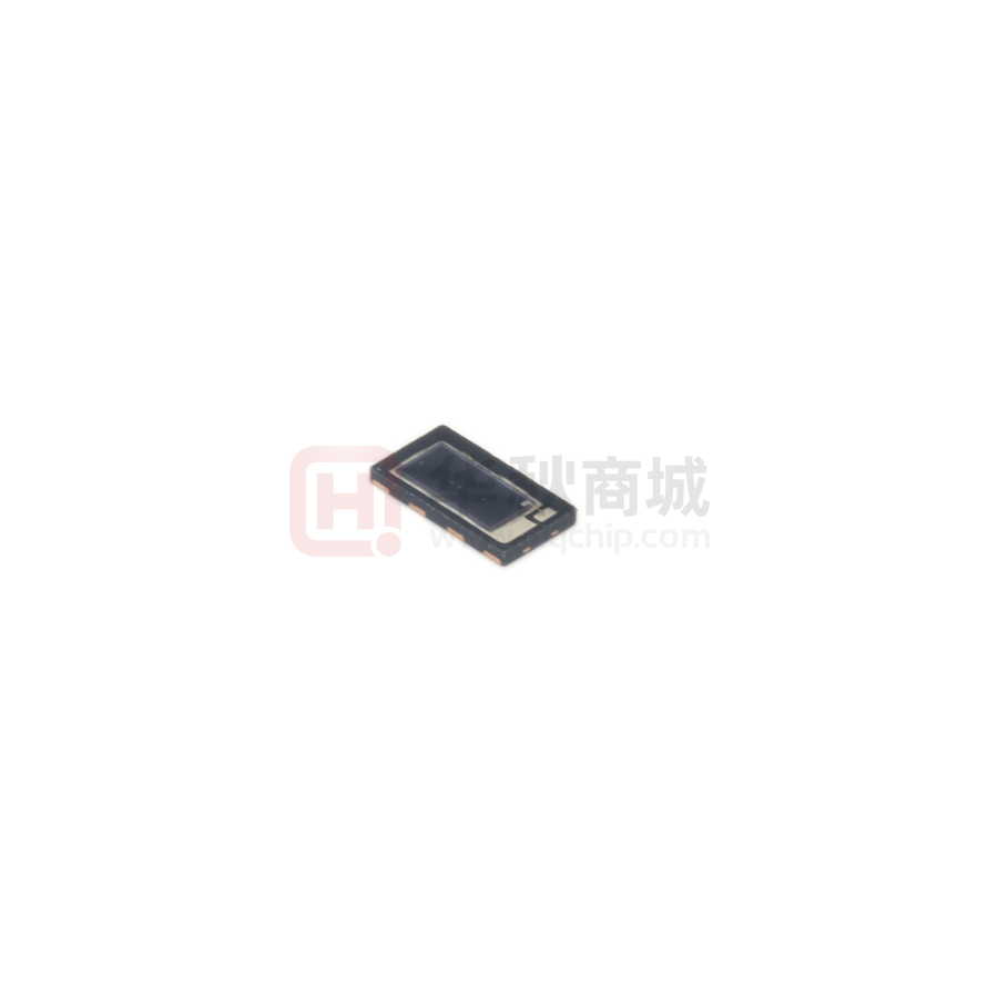
• Package type: surface-mount
• Package form: top view
• Dimensions (L x W x H in mm): 4.8 x 2.5 x 0.48
• Radiant sensitive area (in mm2): 4.5
• 0.48 mm low profile package
• Enhanced sensitivity for visible light
• Suitable for visible and near infrared radiation
• Fast response times
• Angle of half sensitivity: ϕ = ± 65°
• Floor life: 168 h, MSL 3, according to J-STD-020
DESCRIPTION
VEMD8080 is a high speed and high sensitive PIN
photodiode with enhanced sensitivity for visible light. It is a
low profile surface-mount device (SMD) including the chip
with a 4.5 mm2 sensitive area detecting visible and near
infrared radiation.
• Material categorization: for definitions of compliance
please see www.vishay.com/doc?99912
APPLICATIONS
• High speed photo detector
• Wearables
PRODUCT SUMMARY
COMPONENT
VEMD8080
Ira (μA)
ϕ (deg)
λ0.1 (nm)
28
± 65
350 to 1100
Note
• Test conditions see table “Basic Characteristics”
ORDERING INFORMATION
ORDERING CODE
PACKAGING
REMARKS
PACKAGE FORM
VEMD8080
Tape and reel
MOQ: 5000 pcs, 5000 pcs/reel
Top view
Note
• MOQ: minimum order quantity
ABSOLUTE MAXIMUM RATINGS (Tamb = 25 °C, unless otherwise specified)
PARAMETER
SYMBOL
VALUE
Reverse voltage
VR
20
V
Junction temperature
Tj
85
°C
Operating temperature range
Tamb
-40 to +85
°C
Storage temperature range
Tstg
-40 to +85
°C
Tsd
260
°C
RthJA
350
K/W
ESDHBM
≥2
kV
Soldering temperature
TEST CONDITION
According to reflow solder profile Fig. 8
Thermal resistance junction-to-ambient
ESD safety HBM
Rev. 1.0, 24-Apr-2018
± 2000 V, 1.5 kΩ, 100 pF, 3 pulses
UNIT
Document Number: 84565
1
For technical questions, contact: detectortechsupport@vishay.com
THIS DOCUMENT IS SUBJECT TO CHANGE WITHOUT NOTICE. THE PRODUCTS DESCRIBED HEREIN AND THIS DOCUMENT
ARE SUBJECT TO SPECIFIC DISCLAIMERS, SET FORTH AT www.vishay.com/doc?91000
�VEMD8080
www.vishay.com
Vishay Semiconductors
BASIC CHARACTERISTICS (Tamb = 25 °C, unless otherwise specified)
PARAMETER
TEST CONDITION
SYMBOL
MIN.
TYP.
MAX.
UNIT
IF = 50 mA
VF
-
1.2
1.6
V
IR = 100 μA, E = 0
V(BR)
20
-
-
V
VR = 10 V, E = 0
Iro
-
0.2
10
nA
VR = 0 V, f = 1 MHz, E = 0
CD
-
47
-
pF
Forward voltage
Breakdown voltage
Reverse dark current
Diode capacitance
VR = 3 V, f = 1 MHz, E = 0
CD
-
17
40
pF
Open circuit voltage
Ee = 1 mW/cm2, λ = 950 nm
Vo
-
320
-
mV
Temperature coefficient of Vo
Ee = 1 mW/cm2, λ = 950 nm
TKVo
-
-3.0
-
mV/K
Short circuit current
Ee = 1 mW/cm2, λ = 950 nm
Ik
-
32
-
μA
Temperature coefficient of Ik
Ee = 1 mW/cm2, λ = 950 nm
TKIk
-
0.1
-
%/K
Ee = 1 mW/cm2, λ = 850 nm, VR = 5 V
Ira
23
28
33
μA
Ee = 0.25 mW/cm2, λ = 525 nm, VR = 5 V
Ira
3.4
4.4
5.3
μA
ϕ
-
± 65
-
deg
Wavelength of peak sensitivity
λp
-
850
-
nm
Range of spectral bandwidth
λ0.1
-
350 to 1100
-
nm
Reverse light current
Angle of half sensitivity
Rise time
VR = 10 V, RL = 1 kΩ, λ = 830 nm
tr
-
70
-
ns
Fall time
VR = 10 V, RL = 1 kΩ, λ = 830 nm
tf
-
70
-
ns
BASIC CHARACTERISTICS (Tamb = 25 °C, unless otherwise specified)
1.2
VR = 10 V
100
10
1
0.1
0
20
40
60
80
Tamb - Ambient Temperature (°C)
Fig. 1 - Reverse Dark Current vs. Ambient Temperature
Rev. 1.0, 24-Apr-2018
Ira rel - Relative Reverse Light Current
Iro - Reverse Dark Current (nA)
1000
Ee = 1 mW/cm2
λ = 950 nm
VR = 5 V
1.1
1
0.9
0.8
-40
-20
0
20
40
60
80
Tamb - Ambient Temperature (°C)
Fig. 2 - Relative Reverse Light Current vs. Ambient Temperature
Document Number: 84565
2
For technical questions, contact: detectortechsupport@vishay.com
THIS DOCUMENT IS SUBJECT TO CHANGE WITHOUT NOTICE. THE PRODUCTS DESCRIBED HEREIN AND THIS DOCUMENT
ARE SUBJECT TO SPECIFIC DISCLAIMERS, SET FORTH AT www.vishay.com/doc?91000
�VEMD8080
www.vishay.com
Vishay Semiconductors
S(λ)rel - Relative Spectral Sensitivity
VR = 5 V, λ = 950 nm
10
1
0.1
0.01
0.1
Ee - Irradiance
1.0
0.9
0.8
0.7
0.6
0.5
0.4
0.3
0.2
0.1
0
400
1
500
600
700
800
Fig. 3 - Reverse Light Current vs. Irradiance
Fig. 5 - Relative Spectral Sensitivity vs. Wavelength
0°
50
10°
20°
30°
Srpel - Relative Sensitivity
f = 1 MHz, E = 0
Cp - Capacitance (pF)
900 1000 1100
λ - Wavelength (nm)
(mW/cm2)
40
30
20
10
40°
1.0
0.9
50°
0.8
60°
70°
0.7
ϕ - Angular Displacement
Ira - Reverse Light Current (μA)
100
80°
0
0.1
1
10
100
0.6
0.4
0.2
0
VR - Reverse Voltage (V)
Fig. 4 - Diode Capacitance vs. Reverse Voltage
Rev. 1.0, 24-Apr-2018
Fig. 6 - Relative Sensitivity vs. Angular Displacement
Document Number: 84565
3
For technical questions, contact: detectortechsupport@vishay.com
THIS DOCUMENT IS SUBJECT TO CHANGE WITHOUT NOTICE. THE PRODUCTS DESCRIBED HEREIN AND THIS DOCUMENT
ARE SUBJECT TO SPECIFIC DISCLAIMERS, SET FORTH AT www.vishay.com/doc?91000
�VEMD8080
www.vishay.com
Vishay Semiconductors
0.55 (x 8)
PACKAGE DIMENSIONS in millimeters
Footprint
2.38
0.15
0.54 (x 8)
0.29
1.63
2.5
4.8
1.31
1.38
1.31
0.48 ± 0.05
0.5
0.15
2.4
Not indicated tolerances ± 0.1 mm
Pinning top view
1.31
1.38
1.31
PD pin 8
cathode
PD pin 7
cathode
PD pin 6
cathode
PD pin 5
anode
PD pin 1
cathode
PD pin 2
cathode
PD pin 3
cathode
PD pin 4
cathode
4.32
2.02
1.25
2.14
(0.14)
Pinning bottom view
Optical center PD
(0.14)
Drawing number: 6.550-5354.01-4
Issue: 1; 20.04.2018
Rev. 1.0, 24-Apr-2018
PD pin 1
cathode
PD pin 2
cathode
PD pin 3
cathode
PD pin 4
cathode
PD pin 8
cathode
PD pin 7
cathode
PD pin 6
cathode
PD pin 5
anode
Pin 1 marking
Technical drawings
according to DIN
specification.
Document Number: 84565
4
For technical questions, contact: detectortechsupport@vishay.com
THIS DOCUMENT IS SUBJECT TO CHANGE WITHOUT NOTICE. THE PRODUCTS DESCRIBED HEREIN AND THIS DOCUMENT
ARE SUBJECT TO SPECIFIC DISCLAIMERS, SET FORTH AT www.vishay.com/doc?91000
�VEMD8080
www.vishay.com
Vishay Semiconductors
TAPE AND REEL DIMENSIONS in millimeters
Non tolerated dimensions ± 0.1 mm
Reel design is representative for different types
Unreel direction
Re
el Ø
3
0.25
Ø1
0.9
A
Label posted here
12
Ø 1.5
.4
4
Sensor orientation mark pin 1
4
A
(5 : 1)
2
18
Ø 1.5
Drawing-No.: 9.800-5146.01-4
Issue: 1; 20.04.2018
Rev. 1.0, 24-Apr-2018
5.5
1.75
Document Number: 84565
5
For technical questions, contact: detectortechsupport@vishay.com
THIS DOCUMENT IS SUBJECT TO CHANGE WITHOUT NOTICE. THE PRODUCTS DESCRIBED HEREIN AND THIS DOCUMENT
ARE SUBJECT TO SPECIFIC DISCLAIMERS, SET FORTH AT www.vishay.com/doc?91000
�VEMD8080
www.vishay.com
Vishay Semiconductors
SOLDER PROFILE
DRYPACK
Devices are packed in moisture barrier bags (MBB) to
prevent the products from moisture absorption during
transportation and storage. Each bag contains a desiccant.
Axis Title
10000
300
Max. 260 °C
255 °C
240 °C
217 °C
2nd line
Temperature (°C)
250
FLOOR LIFE
245 °C
Time between soldering and removing from MBB must not
exceed the time indicated in J-STD-020:
1000
200
1st line
2nd line
Max. 30 s
150
Max. 120 s
100
Max. 100 s
Max. ramp down 6 °C/s
100
10
0
0
50
100
150
200
250
300
Time (s)
19841-1
Fig. 7 - Lead (Pb)-free Reflow Solder Profile
According to J-STD-020D
Rev. 1.0, 24-Apr-2018
Floor life: 168 h
Conditions: Tamb < 30 °C, RH < 60 %
DRYING
Max. ramp up 3 °C/s
50
Moisture sensitivity: level 3
In case of moisture absorption devices should be
baked before soldering. Conditions see J-STD-020 or
recommended conditions:
192 h at 40 °C (+ 5 °C), RH < 5 %
or
96 h at 60 °C (+ 5 °C), RH < 5 %
Document Number: 84565
6
For technical questions, contact: detectortechsupport@vishay.com
THIS DOCUMENT IS SUBJECT TO CHANGE WITHOUT NOTICE. THE PRODUCTS DESCRIBED HEREIN AND THIS DOCUMENT
ARE SUBJECT TO SPECIFIC DISCLAIMERS, SET FORTH AT www.vishay.com/doc?91000
�Legal Disclaimer Notice
www.vishay.com
Vishay
Disclaimer
ALL PRODUCT, PRODUCT SPECIFICATIONS AND DATA ARE SUBJECT TO CHANGE WITHOUT NOTICE TO IMPROVE
RELIABILITY, FUNCTION OR DESIGN OR OTHERWISE.
Vishay Intertechnology, Inc., its affiliates, agents, and employees, and all persons acting on its or their behalf (collectively,
“Vishay”), disclaim any and all liability for any errors, inaccuracies or incompleteness contained in any datasheet or in any other
disclosure relating to any product.
Vishay makes no warranty, representation or guarantee regarding the suitability of the products for any particular purpose or
the continuing production of any product. To the maximum extent permitted by applicable law, Vishay disclaims (i) any and all
liability arising out of the application or use of any product, (ii) any and all liability, including without limitation special,
consequential or incidental damages, and (iii) any and all implied warranties, including warranties of fitness for particular
purpose, non-infringement and merchantability.
Statements regarding the suitability of products for certain types of applications are based on Vishay’s knowledge of
typical requirements that are often placed on Vishay products in generic applications. Such statements are not binding
statements about the suitability of products for a particular application. It is the customer’s responsibility to validate that a
particular product with the properties described in the product specification is suitable for use in a particular application.
Parameters provided in datasheets and / or specifications may vary in different applications and performance may vary over
time. All operating parameters, including typical parameters, must be validated for each customer application by the customer’s
technical experts. Product specifications do not expand or otherwise modify Vishay’s terms and conditions of purchase,
including but not limited to the warranty expressed therein.
Except as expressly indicated in writing, Vishay products are not designed for use in medical, life-saving, or life-sustaining
applications or for any other application in which the failure of the Vishay product could result in personal injury or death.
Customers using or selling Vishay products not expressly indicated for use in such applications do so at their own risk.
Please contact authorized Vishay personnel to obtain written terms and conditions regarding products designed for
such applications.
No license, express or implied, by estoppel or otherwise, to any intellectual property rights is granted by this document
or by any conduct of Vishay. Product names and markings noted herein may be trademarks of their respective owners.
© 2019 VISHAY INTERTECHNOLOGY, INC. ALL RIGHTS RESERVED
Revision: 01-Jan-2019
1
Document Number: 91000
�