VLMU3500-...-120..
www.vishay.com
Vishay Semiconductors
UV SMD LED With Silicone Lens
FEATURES
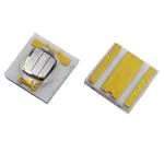
• Ceramic SMT package with silicone lens
• Dimension (L x W x H) in mm: 3.5 x 3.5 x 2.2
• Forward current: up to 700 mA
• Radiant power (typ.): 780 mW at 500 mA,
1037 mW at 700 mA
• Materials:
- Die: InGaN
- Resin: silicone (water clear)
- Leads / terminations finish: gold plated (Au)
DESCRIPTION
• Grouping parameters:
VLMU3500-...-120.. series is a ceramic based high power
UV LED with silicone lens for long life time. The package size
is 3.5 mm x 3.5 mm and the radiant power up to 1250 mW
at 700 mA in a wavelength range of 380 nm to 410 nm.
- Radiant power
PRODUCT GROUP AND PACKAGE DATA
• MSL2 according to J-STD-020
• Product group: LED
• Packaging: MOQ = 100 pieces; 12 mm tape with
100 pieces per reel, Ø 180 mm (7")
- Peak wavelength
- Forward voltage
• Reflow soldering method
• Package: SMD ceramic high power
• Material categorization: for definitions of compliance
please see www.vishay.com/doc?99912
• Product series: high power UV LED
• Angle of half intensity: ± 60°
APPLICATIONS
• Lead-finishing: Au
• Industrial curing
SAFETY ADVICES
• Photocatalytic purification
Depending on the mode of operation, these devices emit
highly concentrated non visible ultraviolet light which can be
hazardous to the human eye. Products which incorporate
these devices have to follow the safety precautions given in
IEC 62471 “Photobiological Safety of Lamps and Lamp
Systems”.
• Poster printing curing
• Counterfeit money detector
• Blood detector
• Nail curing
• Teeth curing
PARTS TABLE
PART
VLMU3500-385-120
COLOR
Ultraviolet
RADIANT POWER
(mW)
MIN.
WAVELENGTH
at
at FORWARD VOLTAGE at
(nm)
(V)
IF
IF
IF TECHNOLOGY
TYP. MAX. (mA) MIN. TYP. MAX. (mA) MIN. TYP. MAX. (mA)
620
780
940
500
380
385
390
500
2.8
3.4
4.0
500
InGaN
VLMU3500-385-120-L Ultraviolet
620
780
940
500
380
385
390
500
2.8
3.4
4.0
500
InGaN
VLMU3500-395-120
Ultraviolet
620
780
940
500
390
395
400
500
2.8
3.4
4.0
500
InGaN
VLMU3500-395-120-L Ultraviolet
620
780
940
500
390
395
400
500
2.8
3.4
4.0
500
InGaN
VLMU3500-405-120
Ultraviolet
620
780
940
500
400
405
410
500
2.8
3.4
4.0
500
InGaN
VLMU3500-405-120-L Ultraviolet
620
780
940
500
400
405
410
500
2.8
3.4
4.0
500
InGaN
Document Number: 84320
1
For technical questions, contact: LED@vishay.com
THIS DOCUMENT IS SUBJECT TO CHANGE WITHOUT NOTICE. THE PRODUCTS DESCRIBED HEREIN AND THIS DOCUMENT
ARE SUBJECT TO SPECIFIC DISCLAIMERS, SET FORTH AT www.vishay.com/doc?91000
Rev. 1.4, 03-Mar-2020
�VLMU3500-...-120..
www.vishay.com
Vishay Semiconductors
ABSOLUTE MAXIMUM RATINGS (Tamb = 25 °C, unless otherwise specified)
VLMU3500-...-120..
SYMBOL
VALUE
UNIT
DC forward current
PARAMETER
IF
700
mA
Power dissipation
PV
2.8
W
ESD
8000
V
Tj
+125
°C
Electrostatic discharge
TEST CONDITION
HBM: MIL-STD-883 C 3B
Junction temperature
Operating temperature range
Tamb
-40 to +85
°C
Storage temperature range
Tstg
-40 to +100
°C
Solder temperature
Tsol
260
°C
RthJS
8
°C/W
Thermal resistance - junction to solder point
OPTICAL AND ELECTRICAL CHARACTERISTICS (Tamb = 25 °C, unless otherwise specified)
VLMU3500-...-120.., ULTRAVIOLET
PARAMETER
Forward voltage
TEST CONDITION
DEVICE TYPE
IF = 500 mA
SYMBOL
MIN.
TYP.
MAX.
UNIT
VF
2.8
3.4
4
V
445
560
675
IF = 350 mA
Radiant power
Radiant intensity
φe
IF = 500 mA
620
780
940
IF = 700 mA
824
1037
1250
IF = 350 mA
-
210
-
-
295
-
-
390
-
IF = 500 mA
le
IF = 700 mA
VLMU3500-385-120..
λp
Peak wavelength
IF = 500 mA
Angle of half intensity
IF = 500 mA
ϕ
VR = 5 V
IR
VLMU3500-395-120..
VLMU3500-405-120..
Reverse current
mW
mW/sr
380
385
390
nm
390
395
400
nm
400
405
410
nm
-
± 60
-
°
-
-
10
μA
Note
• Tolerances: ± 11 % for φe, ± 0.1 V for VF, ± 1 nm for λp
RADIANT POWER CLASSIFICATION (IF = 500 mA)
GROUP
MIN.
MAX.
U062
620
660
U066
660
700
U070
700
740
U074
740
780
U078
780
820
U082
820
860
U086
860
900
U090
900
940
UNIT
mW
PEAK WAVELENGTH CLASSIFICATION (IF = 500 mA)
GROUP
MIN.
MAX.
Q380
380
385
Q385
385
390
Q390
390
395
Q395
395
400
Q400
400
405
Q405
405
410
UNIT
nm
Document Number: 84320
2
For technical questions, contact: LED@vishay.com
THIS DOCUMENT IS SUBJECT TO CHANGE WITHOUT NOTICE. THE PRODUCTS DESCRIBED HEREIN AND THIS DOCUMENT
ARE SUBJECT TO SPECIFIC DISCLAIMERS, SET FORTH AT www.vishay.com/doc?91000
Rev. 1.4, 03-Mar-2020
�VLMU3500-...-120..
www.vishay.com
Vishay Semiconductors
FORWARD VOLTAGE CLASSIFICATION (IF = 500 mA)
MIN.
MAX.
V2830
GROUP
2.8
3.0
V3032
3.0
3.2
V3234
3.2
3.4
V3436
3.4
3.6
V3638
3.6
3.8
V3840
3.8
4.0
UNIT
V
Note
• In order to ensure availability, single groups for radiant intensity, wavelength, and forward voltage will not be orderable. Only one group for
radiant intensity, wavelength, and forward voltage will be shipped in any one reel
MARKING EXAMPLE FOR SELECTION CODE ON LABEL
Selection code: U074Q385V3436
• U074: φe, range 740 mW to 780 mW
• Q385: λp, range 385 nm to 390 nm
• V3436: VF, range 3.4 V to 3.6 V
TYPICAL CHARACTERISTICS (Tamb = 25 °C, unless otherwise specified)
Axis Title
125
100
75
50
25
100
200
300
400
500
600
385 nm
405 nm
40
100
20
0
700
10
340
360
IF - Forward Current (mA)
380
400
0°
Ie, rel - Relative Radiant Intensity
600
500
400
300
200
100
0
1.0
1.5
2.0
2.5
3.0
440
460
Fig. 3 - Relative Spectral Power vs. Wavelength
700
0.5
420
Wavelength (nm)
2nd line
Fig. 1 - Relative Radiant Power vs. Forward Current
0
1000
60
3.5
4.0
10°
20°
30°
40°
1.0
0.9
50°
0.8
60°
70°
0.7
80°
0.6
0.4
0.2
ϕ - Angular Displacement
0
80
1st line
2nd line
150
0
IF - Forward Current (mA)
10000
175
2nd line
Relative Spectral Power (%)
Relative Radiant Power (%)
395 nm
100
200
0
VF - Forward Voltage (V)
Fig. 2 - Forward Current vs. Forward Voltage
Fig. 4 - Relative Intensity vs. Angular Displacement
Document Number: 84320
3
For technical questions, contact: LED@vishay.com
THIS DOCUMENT IS SUBJECT TO CHANGE WITHOUT NOTICE. THE PRODUCTS DESCRIBED HEREIN AND THIS DOCUMENT
ARE SUBJECT TO SPECIFIC DISCLAIMERS, SET FORTH AT www.vishay.com/doc?91000
Rev. 1.4, 03-Mar-2020
�VLMU3500-...-120..
www.vishay.com
Vishay Semiconductors
800
RthJA = 20 °C/W
RthJA = 25 °C/W
700
1000
600
500
400
100
300
200
100
0
10
0
20
40
60
80
10000
6
4
1000
2
1st line
2nd line
900
2nd line
Δλp - Change of Peak Wavelength (nm)
Axis Title
10000
1st line
2nd line
2nd line
IF max. - Maximum Forward Current (mA)
Axis Title
1000
0
-2
100
-4
-6
100 120 140 160
10
-40
-20
0
20
40
60
80
100
Tamb - Ambient Temperature (°C)
2nd line
Tamb - Ambient Temperature (°C)
2nd line
Fig. 5 - Maximum Forward Current vs. Ambient Temperature
Fig. 7 - Change of Peak Wavelength vs. Ambient Temperature
Axis Title
Axis Title
0.6
100
0.4
0.2
0
10
-40
-20
0
20
40
60
80
100
0.2
1000
0.1
1st line
2nd line
0.8
2nd line
ΔVF - Change of Forward Voltage (V)
1000
1st line
2nd line
2nd line
Φe rel - Relative Radiant Flux
1.2
1.0
10000
0.3
10000
1.4
0
-0.1
100
-0.2
-0.3
10
-40
-20
0
20
40
60
80
100
Tamb - Ambient Temperature (°C)
2nd line
Tamb - Ambient Temperature (°C)
2nd line
Fig. 6 - Relative Radiant Flux vs. Ambient Temperature
Fig. 8 - Change of Forward Voltage vs. Ambient Temperature
Document Number: 84320
4
For technical questions, contact: LED@vishay.com
THIS DOCUMENT IS SUBJECT TO CHANGE WITHOUT NOTICE. THE PRODUCTS DESCRIBED HEREIN AND THIS DOCUMENT
ARE SUBJECT TO SPECIFIC DISCLAIMERS, SET FORTH AT www.vishay.com/doc?91000
Rev. 1.4, 03-Mar-2020
�VLMU3500-...-120..
www.vishay.com
Vishay Semiconductors
PACKAGE DIMENSIONS in millimeters
Electrically neutral
thermal pad
3.2
1.3
2.3
3.2
A
Technical drawings
according to DIN
specification
C
Cathode
0.15
1.68
0.54
R1.53
Recommended solder pad footprint
4.1
3.3
2.3
3.5
1.3
3.3
3.5
0.5
C
A
Not indicated tolerances ± 0.13
Drawing-No.: 6.541-5107.01-4
Issue: 3VK; 26.11.19
WIRING
ZD
LED
Fig. 9 - Wiring Diagram
Document Number: 84320
5
For technical questions, contact: LED@vishay.com
THIS DOCUMENT IS SUBJECT TO CHANGE WITHOUT NOTICE. THE PRODUCTS DESCRIBED HEREIN AND THIS DOCUMENT
ARE SUBJECT TO SPECIFIC DISCLAIMERS, SET FORTH AT www.vishay.com/doc?91000
Rev. 1.4, 03-Mar-2020
�VLMU3500-...-120..
www.vishay.com
Vishay Semiconductors
TAPE AND REEL DIMENSIONS in millimeters
Reel
Unreel direction
60.2 ± 0.5
X
Ø 178 ± 1
Tape position
coming out from reel
100 pcs/reel for VLMU35..-...-120
1000 pcs/reel for VLMU35..-...-120-L
Ø 13.5
Label posted here
16 ± 1
technical drawings
according to DIN
specifications
Leader and trailer tape
Empty (160 mm min.)
Parts mounted
Direction of pulling out
4 ± 0.1
2 ± 0.1
X 2:1
Ø 1.55 ± 0.05
C
5.5 ± 0.05
12 ± 0.3
1.75 ± 0.1
Empty (400 mm min.)
8 ± 0.1
Ø 1.5 min.
A
2.5
Drawing-No.: 9.800-5130.01-4
Issue: 2VK; 20.02.2020
Document Number: 84320
6
For technical questions, contact: LED@vishay.com
THIS DOCUMENT IS SUBJECT TO CHANGE WITHOUT NOTICE. THE PRODUCTS DESCRIBED HEREIN AND THIS DOCUMENT
ARE SUBJECT TO SPECIFIC DISCLAIMERS, SET FORTH AT www.vishay.com/doc?91000
Rev. 1.4, 03-Mar-2020
�VLMU3500-...-120..
www.vishay.com
Vishay Semiconductors
HANDLING RECOMMENDATIONS
BAR CODE PRODUCT LABEL (example only)
In order to achieve excellent lifetime, the package of these
UV-LEDs consists of a ceramic substrate in combination
with a UV stable silicone as lens material. Compared to
standard materials silicone is generally softer and it tends
more to attract dust:
A
N
B
• Minimize the level of dirt and dust particles in contact with
the LED
Part No: VLMU3500-385-120
C
• Small amounts of particles on the LEDs, although
noticeable from a cosmetic point of view, do not affect the
performance in terms of brightness, reliability and quality
E
QTY: 100
e4
SelCode: U074Q385V3436
Origin CHINA Machine:01
PTC: 29
D
G
F
Lot1: XXXXXXXXXX
VISHAY
Lot2:
Batch: YYYYWWCCPP
Region: 2146 SL: 0010
H/F
Serial#: XXXXXXXXXXXX
Operator:
ChkD:
H
• If cleaning is required, a short rinsing with isopropyl
alcohol, not longer than 15 seconds, is recommended. Do
not use ultrasonic cleaning, it may damage the LED
A. 2D barcode
B. Par No: Vishay part number
• Do not apply mechanical stress on the silicone lens
C. QTY: quantity
• Avoid any piercing of the silicone lens by sharp objects
D. SelCode: selection bin code
• It is recommended to use a suitable pick and place tool for
the removal of the LED from blister tape without applying
stress to the lens. The recess of the pick-up needle has to
be larger than the silicone lens
E. Country of origin
• For manual handling using tweezers make sure that the
LED will be touched carefully at the sidewall of the ceramic
substrate, but not at the silicone lens
K
L
M
F. PTC: production plant code
G. Termination finish
H. Region code
I. Serial#: serial number
K. Batch number: year, week, country code, plant code
L. SL: Sales location
SOLDERING PROFILE
M. Environmental symbols: RoHS, lead (Pb)-free, halogen
free
IR Reflow Soldering Profile for Lead (Pb)-Free Soldering
Preconditioning according to JEDEC level 2
n. Lot numbers
300
max. 260 °C
245 °C
255 °C
240 °C
217 °C
250
Temperature (°C)
I
The reel is packed in an anti-humidity bag to protect the
devices from absorbing moisture during transportation and
storage.
200
max. 30 s
150
max. 100 s
max. 120 s
DRY PACKING
Aluminum bag
100
max. ramp up 3 °C/s
50
max. ramp down 6 °C/s
Label
0
0
50
19885-2
100
150
Time (s)
200
250
300
max. 2 cycles allowed
Fig. 10 - Vishay Lead (Pb)-Free Reflow Soldering Profile
(according to J-STD-020C)
Reel
15973
FINAL PACKING
The sealed reel is packed into a cardboard box. A secondary
cardboard box is used for shipping purposes.
Document Number: 84320
7
For technical questions, contact: LED@vishay.com
THIS DOCUMENT IS SUBJECT TO CHANGE WITHOUT NOTICE. THE PRODUCTS DESCRIBED HEREIN AND THIS DOCUMENT
ARE SUBJECT TO SPECIFIC DISCLAIMERS, SET FORTH AT www.vishay.com/doc?91000
Rev. 1.4, 03-Mar-2020
�VLMU3500-...-120..
www.vishay.com
Vishay Semiconductors
RECOMMENDED METHOD OF STORAGE
ESD PRECAUTION
Dry box storage is recommended as soon as the aluminum
bag has been opened to prevent moisture absorption. The
following conditions should be observed, if dry boxes are
not available:
Proper storage and handling procedures should be followed
to prevent ESD damage to the devices especially when they
are removed from the antistatic shielding bag. Electrostatic
sensitive devices warning labels are on the packaging.
• Storage temperature 10 °C to 30 °C
• Storage humidity ≤ 60 % RH max.
After more than 1 year under these conditions moisture
content will be too high for reflow soldering.
In case of moisture absorption, the devices will recover to
the former condition by drying under the following condition:
VISHAY SEMICONDUCTORS STANDARD
BAR CODE LABELS
The Vishay Semiconductors standard bar code labels are
printed at final packing areas. The labels are on each
packing unit and contain Vishay Semiconductors specific
data.
192 h at 40 °C + 5 °C / - 0 °C and < 5 % RH (dry air /
nitrogen) or
24 h at 60 °C + 5 °C and < 5 % RH for all device containers
or
24 h at 100 °C + 5 °C not suitable for reel or tubes.
An EIA JEDEC® standard JESD22-A112 level 2 label is
included on all dry bags.
17028
Example of JESD22-A112 level 2 label
Document Number: 84320
8
For technical questions, contact: LED@vishay.com
THIS DOCUMENT IS SUBJECT TO CHANGE WITHOUT NOTICE. THE PRODUCTS DESCRIBED HEREIN AND THIS DOCUMENT
ARE SUBJECT TO SPECIFIC DISCLAIMERS, SET FORTH AT www.vishay.com/doc?91000
Rev. 1.4, 03-Mar-2020
�Legal Disclaimer Notice
www.vishay.com
Vishay
Disclaimer
ALL PRODUCT, PRODUCT SPECIFICATIONS AND DATA ARE SUBJECT TO CHANGE WITHOUT NOTICE TO IMPROVE
RELIABILITY, FUNCTION OR DESIGN OR OTHERWISE.
Vishay Intertechnology, Inc., its affiliates, agents, and employees, and all persons acting on its or their behalf (collectively,
“Vishay”), disclaim any and all liability for any errors, inaccuracies or incompleteness contained in any datasheet or in any other
disclosure relating to any product.
Vishay makes no warranty, representation or guarantee regarding the suitability of the products for any particular purpose or
the continuing production of any product. To the maximum extent permitted by applicable law, Vishay disclaims (i) any and all
liability arising out of the application or use of any product, (ii) any and all liability, including without limitation special,
consequential or incidental damages, and (iii) any and all implied warranties, including warranties of fitness for particular
purpose, non-infringement and merchantability.
Statements regarding the suitability of products for certain types of applications are based on Vishay's knowledge of typical
requirements that are often placed on Vishay products in generic applications. Such statements are not binding statements
about the suitability of products for a particular application. It is the customer's responsibility to validate that a particular product
with the properties described in the product specification is suitable for use in a particular application. Parameters provided in
datasheets and / or specifications may vary in different applications and performance may vary over time. All operating
parameters, including typical parameters, must be validated for each customer application by the customer's technical experts.
Product specifications do not expand or otherwise modify Vishay's terms and conditions of purchase, including but not limited
to the warranty expressed therein.
Hyperlinks included in this datasheet may direct users to third-party websites. These links are provided as a convenience and
for informational purposes only. Inclusion of these hyperlinks does not constitute an endorsement or an approval by Vishay of
any of the products, services or opinions of the corporation, organization or individual associated with the third-party website.
Vishay disclaims any and all liability and bears no responsibility for the accuracy, legality or content of the third-party website
or for that of subsequent links.
Except as expressly indicated in writing, Vishay products are not designed for use in medical, life-saving, or life-sustaining
applications or for any other application in which the failure of the Vishay product could result in personal injury or death.
Customers using or selling Vishay products not expressly indicated for use in such applications do so at their own risk. Please
contact authorized Vishay personnel to obtain written terms and conditions regarding products designed for such applications.
No license, express or implied, by estoppel or otherwise, to any intellectual property rights is granted by this document or by
any conduct of Vishay. Product names and markings noted herein may be trademarks of their respective owners.
© 2022 VISHAY INTERTECHNOLOGY, INC. ALL RIGHTS RESERVED
Revision: 01-Jan-2022
1
Document Number: 91000
�