VLMW1300
www.vishay.com
Vishay Semiconductors
Highbright 0603 ChipLED
FEATURES
• High efficient InGaN technology
• Super thin ChipLED with exceptional brightness
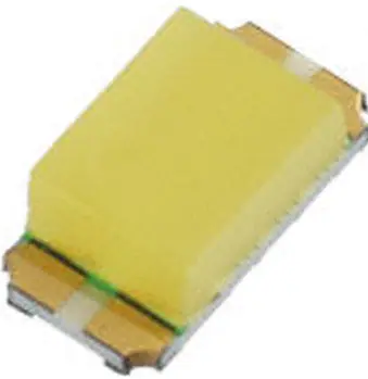
1.6 mm x 0.8 mm x 0.55 mm (L x W x H)
• High reliability PCB based
• Temperature range -20 °C to +80 °C
• Chromaticity coordinate categorized according
to CIE 1931 per packing unit
• Typical color temperature 7000 K
• EIA standard package
DESCRIPTION
• Compatible to IR reflow soldering
The new 0603 ChipLED series have been designed in the
smallest SMD package. This innovative 0603 ChipLED
technology opens the way to
• Available on 7" diameter reel
• Preconditioning according to JEDEC® level 2a
• Smaller products of higher performance
• ESD-sensitive device
• More design in flexibility
• Material categorization: for definitions of compliance
please see www.vishay.com/doc?99912
• Enhanced applications
The 0603 LED is an obvious solution for small-scale
products that are expected to work reliably in an arduous
environment.
APPLICATIONS
• Telecommunication:
telephone and fax
This package is filled with a mixture of epoxy and yellow
converter.
indicator
and
backlighting
in
• Backlighting for audio and video equipment
• Backlighting in office equipment
This yellow converter converts the blue emission partially to
yellow, which mixes the remaining blue to give white.
• Indoor and outdoor message boards
• Flat backlight for LCDs, switches, and symbols
PRODUCT GROUP AND PACKAGE DATA
• Product group: LED
• Package: SMD 0603 ChipLED
• Product series: standard
• Angle of half intensity: ± 65°
PARTS TABLE
PART
VLMW1300-GS08
COLOR
White
LUMINOUS INTENSITY
COORDINATE
FORWARD VOLTAGE
at IF
at IF
at IF
(mcd)
(x, y)
(V)
TECHNOLOGY
(mA)
(mA)
(mA)
MIN.
TYP.
MAX.
MIN. TYP. MAX.
MIN. TYP. MAX.
45
-
180
5
-
0.294,
0.286
-
5
2.70
-
3.15
5
InGaN/
yellow converter
ABSOLUTE MAXIMUM RATINGS (Tamb = 25 °C, unless otherwise specified)
VLMW1300
PARAMETER
DC forward current
Surge forward current
Power dissipation
TEST CONDITION
SYMBOL
VALUE
UNIT
Tamb ≤ 25 °C
IF
20
mA
tp ≤ 10 μs
IFSM
0.1
A
PV
70
mW
Operating temperature range
Tamb
-20 to +80
°C
Storage temperature range
Tstg
-55 to +105
°C
RthJA
550
K/W
Thermal resistance junction/ambient
Rev. 1.2, 22-Sep-14
Document Number: 82435
1
For technical questions, contact: LED@vishay.com
THIS DOCUMENT IS SUBJECT TO CHANGE WITHOUT NOTICE. THE PRODUCTS DESCRIBED HEREIN AND THIS DOCUMENT
ARE SUBJECT TO SPECIFIC DISCLAIMERS, SET FORTH AT www.vishay.com/doc?91000
�VLMW1300
www.vishay.com
Vishay Semiconductors
OPTICAL AND ELECTRICAL CHARACTERISTICS (Tamb = 25 °C, unless otherwise specified)
VLMW1300, WHITE
PARAMETER
TEST CONDITION
SYMBOL
MIN.
TYP.
MAX.
UNIT
Luminous intensity
IF = 5 mA
IV
45
-
180
mcd
Chromatically coordinate x acc. to CIE 1931
IF = 5 mA
x
-
0.294
-
Chromatically coordinate y acc. to CIE 1931
IF = 5 mA
y
-
0.286
-
Angle of half intensity
IF = 5 mA
ϕ
-
± 65
-
Forward voltage
IF = 5 mA
VF
2.70
-
3.15
V
Reverse current (1)
VR = 5 V
IR
-
10
-
μA
deg
Note
(1) Driving the LED in reverse direction is suitable for short term application
LUMINOUS INTENSITY CLASSIFICATION
GROUP
LUMINOUS INTENSITY (mcd)
at 5 mA
FORWARD VOLTAGE CLASSIFICATION
GROUP
FORWARD VOLTAGE (V)
MIN.
MAX.
2.85
MIN.
MAX.
A
2.7
P
45
71
B
2.85
3.0
Q
71
112
C
3.0
3.15
R
112
180
Note
• Luminous intensity is tested at a current pulse duration of 25 ms
and an accuracy of ± 15 %.
The above type numbers represent the order groups which
include only a few brightness groups. Only one group will be
shipped on each reel (there will be no mixing of two groups on
each reel). In order to ensure availability, single brightness
groups will not be orderable.
In a similar manner for colors where wavelength groups are
measured and binned, single wavelength groups will be shipped
in any one reel.
In order to ensure availability, single wavelength groups will not
be orderable.
Note
• Forward voltage is measured with a tolerance of ± 0.1 V.
CHROMATICITY COORDINATED GROUPS FOR WHITE SMD LED
S1
S2
S3
X
Y
X
Y
0.274
0.226
0.294
0.286
0.274
0.258
0.294
0.319
0.294
0.286
0.314
0.347
0.294
0.254
0.314
0.315
0.274
0.258
0.314
0.282
0.274
0.291
0.314
0.315
0.294
0.319
0.334
0.343
0.294
0.286
0.334
0.311
0.294
0.254
0.314
0.315
0.294
0.286
0.314
0.347
0.314
0.315
0.334
0.376
0.314
0.282
0.334
0.343
S4
S5
S6
Note
• Chromaticity coordinate groups are tested at a current pulse duration of 25 ms and a tolerance of ± 0.01.
Rev. 1.2, 22-Sep-14
Document Number: 82435
2
For technical questions, contact: LED@vishay.com
THIS DOCUMENT IS SUBJECT TO CHANGE WITHOUT NOTICE. THE PRODUCTS DESCRIBED HEREIN AND THIS DOCUMENT
ARE SUBJECT TO SPECIFIC DISCLAIMERS, SET FORTH AT www.vishay.com/doc?91000
�VLMW1300
www.vishay.com
Vishay Semiconductors
TYPICAL CHARACTERISTICS (Tamb = 25 °C, unless otherwise specified)
4
Relative Luminous Intensity
Normalized at 5 mA
IF - Forward Current (A)
25
20
15
10
5
3
2
1
0
0
0
20
40
60
80
100
0
10
Tamb Ambient Temperature (°C)
Fig. 1 - Forward Current vs. Ambient Temperature
Irel - Relative Luminous Intensity
Irel - Relative Intensity
0.8
0.7
0.6
0.5
0.4
0.3
0.2
0.1
1
0.1
0
400 450 500 550 600 650 700 750 800
0
λ - Wavelength (nm)
10
20
30
40
50
60
70
80
Tamb - Ambient Temperature (°C)
Fig. 2 - Relative Intensity vs. Wavelength
Fig. 5 - Relative Luminous Intensity vs. Ambient Temperature
50
0.40
y-Coordinates of Colorgroups
IF - Forward Current (mA)
40
10
0.9
40
30
20
10
3.0
3.5
4.0
4.5
5.0
VF - Forward Voltage (V)
Fig. 3 - Forward Current vs. Forward Voltage
Rev. 1.2, 22-Sep-14
30
Fig. 4 - Relative Luminous Intensity vs. Forward Current
1.0
0
2.5
20
IF - Forward Current (mA)
0.38
0.36
S6
0.34
0.32
S4
S5
0.30
S2
0.28
0.26
S3
S1
0.24
0.22
0.20
0.25
0.27
0.29
0.31
0.33
0.35
x-Coordinates of Colorgroups
Fig. 6 - Coordinates of Colorgroups
Document Number: 82435
3
For technical questions, contact: LED@vishay.com
THIS DOCUMENT IS SUBJECT TO CHANGE WITHOUT NOTICE. THE PRODUCTS DESCRIBED HEREIN AND THIS DOCUMENT
ARE SUBJECT TO SPECIFIC DISCLAIMERS, SET FORTH AT www.vishay.com/doc?91000
�VLMW1300
www.vishay.com
10°
20°
30°
40°
1.0
50°
0.9
60°
0.8
70°
0.7
80°
0.6
0.4
0.2
ϕ - Angular Displacement
Irel - Relative Luminous Intensity
0°
Vishay Semiconductors
0
Fig. 7 - Relative Luminous Intensity vs. Angular Displacement
Ø 60 ± 1
Ø 178 ± 2
Ø 13
REEL DIMENSIONS in millimeters
9.4 ± 1.5
Drawing-No.: 9.800-5122.01-4
Issue: 2; 03.11.11
22611
Rev. 1.2, 22-Sep-14
technical drawings
according to DIN
specifications
Document Number: 82435
4
For technical questions, contact: LED@vishay.com
THIS DOCUMENT IS SUBJECT TO CHANGE WITHOUT NOTICE. THE PRODUCTS DESCRIBED HEREIN AND THIS DOCUMENT
ARE SUBJECT TO SPECIFIC DISCLAIMERS, SET FORTH AT www.vishay.com/doc?91000
�VLMW1300
www.vishay.com
Vishay Semiconductors
TAPE DIMENSIONS in millimeters
0.25
0.7
B - B (5:1)
8
+ 0.3
- 0.1
1.75 ± 0.1
B
B
Ø 1.55 ± 0.05
Ø 0.5
2 ± 0.05
4 ± 0.1
4 ± 0.1
User feed direction
Cathode
3.5 ± 0.05
technical drawings
according to DIN
specifications
Drawing-No.: 9.700-5385.01-4
Issue: 1; 17.10.11
22612
Rev. 1.2, 22-Sep-14
Document Number: 82435
5
For technical questions, contact: LED@vishay.com
THIS DOCUMENT IS SUBJECT TO CHANGE WITHOUT NOTICE. THE PRODUCTS DESCRIBED HEREIN AND THIS DOCUMENT
ARE SUBJECT TO SPECIFIC DISCLAIMERS, SET FORTH AT www.vishay.com/doc?91000
�VLMW1300
www.vishay.com
Vishay Semiconductors
PACKAGE DIMENSIONS in millimeters
0.3
0.3
0.8
0.77
Recommended solder
pad footprint
0.8
2.3
0.28
0.55
1.1
0.8
0.3
Cathode
1.6
technical drawings
according to DIN
specifications
Not indicated tolerances ± 0.2
Drawing-No.: 6.541-5091.01-4
Issue: 1; 17.10.11
22613
SOLDERING PROFILE
IR Reflow Soldering Profile for lead (Pb)-free Soldering
Preconditioning acc. to JEDEC Level 2a
300
Temperature (°C)
max. 260 °C
245 °C
255
255 °C
240 °C
217 °C
250
200
max. 30 s
150
max. 100 s
max. 120 s
100
max. Ramp Up 3 °C/s
50
max. Ramp Down 6 °C/s
0
0
50
100
150
Time (s)
200
250
300
max. 2 cycles allowed
Fig. 8 - Vishay Lead (Pb)-free Reflow Soldering Profile
(according to J-STD-020C)
Rev. 1.2, 22-Sep-14
Document Number: 82435
6
For technical questions, contact: LED@vishay.com
THIS DOCUMENT IS SUBJECT TO CHANGE WITHOUT NOTICE. THE PRODUCTS DESCRIBED HEREIN AND THIS DOCUMENT
ARE SUBJECT TO SPECIFIC DISCLAIMERS, SET FORTH AT www.vishay.com/doc?91000
�VLMW1300
www.vishay.com
Vishay Semiconductors
BAR CODE PRODUCT LABEL (Example)
RECOMMENDED METHOD OF STORAGE
Dry box storage is recommended as soon as the aluminum
bag has been opened to prevent moisture absorption. The
following conditions should be observed, if dry boxes are
not available:
A
B
C
D
• Storage temperature 10 °C to 30 °C
L
E
I
G
F
H
M
K
A. 2D barcode
B. PartNo = Vishay part number
C. QTY = Quantity
D. SelCode = selection code (binning)
E. PTC = Code of manufacturing plant
F. Batch = date code: year / week / plant code
G. Region code
H. SL = sales location
I. Terminations finishing
J. Lead (Pb)-free symbol
K. Halogen-free symbol
L. RoHS symbol
• Storage humidity ≤ 60 % RH max.
After more than 672 h under these conditions moisture
content will be too high for reflow soldering.
In case of moisture absorption, the devices will recover to
the former condition by drying under the following condition:
192 h at 40 °C + 5 °C / - 0 °C and < 5 % RH (dry air/nitrogen)
or
96 h at 60 °C + 5 °C and < 5 % RH for all device containers
or
24 h at 100 °C + 5 °C not suitable for reel or tubes.
An EIA JEDEC standard JESD22-A112 level 2a label is
included on all dry bags.
L E V E L
CAUTION
This bag contains
MOISTURE –SENSITIVE DEVICES
2a
DRY PACKING
1. Shelf life in sealed bag 12 months at
很抱歉,暂时无法提供与“VLMW1300-GS08”相匹配的价格&库存,您可以联系我们找货
免费人工找货- 国内价格
- 1+1.09230
- 200+0.84040
- 1500+0.73040
- 3000+0.67980
- 国内价格
- 10+0.60424
- 50+0.55975
- 200+0.52268
- 600+0.48561
- 1500+0.45596
- 3000+0.43742