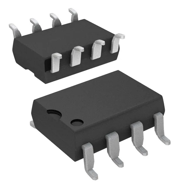
VO1263AAC, VO1263AACTR, VO1263AB
www.vishay.com
Vishay Semiconductors
Dual Photovoltaic MOSFET Driver Solid-State Relay
DIP
8
7
6
5
1
2
3
4
FEATURES
•
•
•
•
•
•
SMD
- Control 1
- Output 1
+ Control 1
+ Output 1
- Control 2
- Output 2
+ Control 2
+ Output 2
High open circuit voltage, up to 14.6 V typical
High short circuit current, up to 42 μA typical
Isolation test voltage 5300 VRMS
Logic compatible input
High reliability
Material categorization: for definitions of
compliance please see www.vishay.com/doc?99912
APPLICATIONS
•
•
•
•
•
•
•
i179034_2
DESIGN SUPPORT TOOLS AVAILABLE
Related
Documents
High side driver
Solid-state relays
Floating power supply
Power control
Data acquisition
ATE
Isolated switching
DESCRIPTION
AGENCY APPROVALS
The VO1263AB and VO1263AAC photovoltaic MOSFET
driver consists of two LEDs optically coupled to two
photodiode arrays. The photodiode array provides a floating
source with adequate voltage and current to drive high
power MOSFET transistors. Optical coupling provides a
high I/O isolation voltage. In order to turn the MOSFET off,
an external resistance (gate-to-source) is required for gate
discharge.
• UL
• DIN EN 60747-5 (VDE 0884-5)
• BSI
• CQC
• FIMKO
ORDERING INFORMATION
V
O
1
2
6
PART NUMBER
3
#
#
ELECTR.
VARIATION
#
PACKAGE
CONFIG.
PACKAGE
T
DIP
R
TAPE AND
REEL
7.62 mm
SMD
> 0.1 mm
UL, VDE, BSI, CQC, FIMKO
SMD-8
VO1263AAC
SMD-8, tape and reel
VO1263AACTR
DIP-8
VO1263AB
ABSOLUTE MAXIMUM RATINGS (Tamb = 25 °C, unless otherwise specified)
PARAMETER
TEST CONDITION
SYMBOL
VALUE
UNIT
LED input ratings reverse voltage
IR ≤ 10 μA
IF
50
mA
VR
5.0
Photodiode array reverse voltage
IR ≤ 2.0 μA
VR
100
V
V
Tamb
-40 to +100
°C
Tstg
-40 to +150
°C
Tsld
270
°C
SSR
LED input ratings continuous forward current
Ambient operating temperature range
Storage temperature range
Pin soldering temperature
t = 7.0 s max.
Note
• Stresses in excess of the absolute maximum ratings can cause permanent damage to the device. Functional operation of the device is not
implied at these or any other conditions in excess of those given in the operational sections of this document. Exposure to absolute
maximum ratings for extended periods of the time can adversely affect reliability
Rev. 2.0, 15-Mar-2019
Document Number: 84639
1
For technical questions, contact: optocoupleranswers@vishay.com
THIS DOCUMENT IS SUBJECT TO CHANGE WITHOUT NOTICE. THE PRODUCTS DESCRIBED HEREIN AND THIS DOCUMENT
ARE SUBJECT TO SPECIFIC DISCLAIMERS, SET FORTH AT www.vishay.com/doc?91000
�VO1263AAC, VO1263AACTR, VO1263AB
www.vishay.com
Vishay Semiconductors
ELECTRICAL CHARACTERISTICS (Tamb = 25 °C, unless otherwise specified)
PARAMETER
TEST CONDITION
SYMBOL
MIN.
TYP.
MAX.
UNIT
IF = 10 mA
VF
1.2
1.3
1.6
V
V
LED forward voltage
Detector reverse voltage
Open circuit voltage (pins 5, 6 or 7, 8)
Short circuit current (pins 5, 6 or 7, 8)
IR = 2.0 μA
VR(PDA)
-
350
-
IF = 5.0 mA
VOC
-
13.73
-
V
IF = 10 mA
VOC
10.3
14.27
16.5
V
IF = 15 mA
VOC
-
14.50
-
V
IF = 20 mA
VOC
-
14.70
-
V
IF = 30 mA
VOC
-
14.94
-
V
IF = 5.0 mA
ISC
2.7
4.47
-
μA
IF = 10 mA
ISC
7
9.8
-
μA
μA
IF = 15 mA
ISC
11
15.33
-
IF = 20 mA
ISC
15
20.97
-
μA
IF = 30 mA
ISC
21
32.4
-
μA
Note
• Minimum and maximum values are testing requirements. Typical values are characteristics of the device and are the result of engineering
evaluations. Typical values are for information only and are not part of the testing requirements
SWITCHING CHARACTERISTICS (Tamb = 25 °C, unless otherwise specified)
PARAMETER
TEST CONDITION
SYMBOL
MIN.
TYP.
MAX.
UNIT
Turn-on time
IF = 20 mA (1)
ton
-
16
-
μs
Turn-off time
IF = 20 mA (1)
toff
-
472
-
μs
Note
f = 1.0 kHz, pulse width = 100 μs, load (RL) = 1.0 MΩ, 15 pF; measured at 90 % rated voltage (ton), 10 % rated voltage (toff). Actuation speed
depends upon the external ton and toff circuitry and the capacitance of the MOSFET
(1)
SAFETY AND INSULATION RATINGS
PARAMETER
TEST CONDITION
SYMBOL
VALUE
Climatic classification
According to IEC 68 part 1
40 / 100 / 21
Pollution degree
According to DIN VDE 0109
2
Comparative tracking index
UNIT
Insulation group IIIa
CTI
175
Maximum rated withstanding isolation voltage
According to UL1577, t = 1 min
VISO
5300
VRMS
Maximum transient isolation voltage
According to DIN EN 60747-5-5
VIOTM
8000
Vpeak
Maximum repetitive peak isolation voltage
According to DIN EN 60747-5-5
VIORM
890
Vpeak
Output safety power
PSO
700
mW
Input safety current
ISI
300
mA
Input safety temperature
TS
175
°C
≥7
mm
≥7
mm
Creepage distance
Clearance distance
DIP-8, SMD-8
Note
• This optocoupler is suitable for “safe electrical insulation” only within the safety ratings. Compliance with the safety ratings shall be ensured
by means of suitable protective circuits
Rev. 2.0, 15-Mar-2019
Document Number: 84639
2
For technical questions, contact: optocoupleranswers@vishay.com
THIS DOCUMENT IS SUBJECT TO CHANGE WITHOUT NOTICE. THE PRODUCTS DESCRIBED HEREIN AND THIS DOCUMENT
ARE SUBJECT TO SPECIFIC DISCLAIMERS, SET FORTH AT www.vishay.com/doc?91000
�VO1263AAC, VO1263AACTR, VO1263AB
www.vishay.com
Vishay Semiconductors
FUNCTIONAL DESCRIPTION
Fig. 1 outlines the IV characteristics of the illuminated photodiode array (PDA). For operation at voltages below VOC, the PDA
acts as a nearly constant current source. The actual region of operation depends upon the load.
The amount of current applied to the LED (pins 1 and 2 or 3 and 4) determines the amount of light produced for the PDA. For
high temperature operation, more LED current may be required.
TYPICAL CHARACTERISTICS (Tamb = 25 °C, unless otherwise specified)
60
100 °C
IF = 30 mA
30
25
Short Circuit Current (μA)
Short Circuit Current (μA)
35
IF = 20 mA
20
IF = 15 mA
15
IF = 10 mA
10
IF = 5 mA
5
50
25 °C
40
- 40 °C
30
20
10
IF = 2 mA
0
0
0
3
6
9
12
0
15
Open Circuit Voltage (V)
20
30
40
50
LED Forward Current (mA)
Fig. 1 - Short Circuit Current vs. Open Circuit Voltage
Fig. 3 - Short Circuit Current vs. LED Forward Current
50
16
RL = 10 MΩ
Short Circuit Current (μA)
14
Output Voltage (V)
10
RL = 5 MΩ
12
RL = 2 MΩ
10
RL = 500 kΩ
8
6
RL = 100 kΩ
4
2
40
IF = 30 mA
30
IF = 20 mA
20
IF = 15 mA
IF = 10 mA
10
IF = 5 mA
0
0
0
10
20
30
40
LED Forward Current (mA)
Fig. 2 - Output Voltage vs-LED Current
Rev. 2.0, 15-Mar-2019
50
-40
-20
0
20
40
60
80
100
Tamb - Ambient Temperature (°C)
Fig. 4 - Short Circuit Current vs. Ambient Temperature
Document Number: 84639
3
For technical questions, contact: optocoupleranswers@vishay.com
THIS DOCUMENT IS SUBJECT TO CHANGE WITHOUT NOTICE. THE PRODUCTS DESCRIBED HEREIN AND THIS DOCUMENT
ARE SUBJECT TO SPECIFIC DISCLAIMERS, SET FORTH AT www.vishay.com/doc?91000
�VO1263AAC, VO1263AACTR, VO1263AB
www.vishay.com
Vishay Semiconductors
2.0
16
IF = 30 mA
IF = 50 mA
IF = 20 mA
14
IF = 10 mA
12
IF = 5 mA
10
Normalized Turn-On Time
Open Circuit Voltage (V)
18
1.8
IF = 5 mA
IL = 50 mA
1.6
1.4
1.2
1.0
0.8
0.6
0.4
0.2
8
Normalized to Tamb = 25 °C
0
-40
-20
0
20
40
60
80
100
-40
Tamb - Ambient Temperature (°C)
Fig. 5 - Open Circuit Voltage vs. Ambient Temperature
20
40
60
80
100
2.0
IF = 30 mA
1.5
IF = 20 mA
1.4
IF = 2 mA
IF = 5 mA
1.3
IF = 10 mA
1.2
IF = 15 mA
1.1
Normalized Turn-Off Time
LED Forward Voltage (V)
0
Fig. 8 - Normalized Turn-On Time vs. Ambient Temperature
1.6
1.8
IF = 5 mA
IL = 50 mA
1.6
1.4
1.2
1.0
0.8
0.6
0.4
0.2
1
Normalized to Tamb = 25 °C
0
-40
-20
0
20
40
60
80
100
-40
Tamb - Ambient Temperature (°C)
Fig. 6 - LED Forward Voltage vs. Ambient Temperature
-20
0
20
40
60
80
100
Tamb - Ambient Temperature (°C)
Fig. 9 - Normalized Turn-Off Time vs. Ambient Temperature
100
2.0
IF = 0 mA
IL = 50 mA
T = 100 °C
10
Turn-On Time (ms)
Off-State Leakage Current (nA)
-20
Tamb - Ambient Temperature (°C)
T = 25 °C
1
0.1
1.5
T = 100 °C
1.0
T = 25 °C
0.5
T = -40 °C
T = -40 °C
0.01
0
0
50
100
150
200
VL - Load Voltage (V)
Fig. 7 - Leakage Current vs. Load Voltage
Rev. 2.0, 15-Mar-2019
0
10
20
30
40
50
IF - Forward Current (mA)
Fig. 10 - Turn-On Time vs. Forward Current
Document Number: 84639
4
For technical questions, contact: optocoupleranswers@vishay.com
THIS DOCUMENT IS SUBJECT TO CHANGE WITHOUT NOTICE. THE PRODUCTS DESCRIBED HEREIN AND THIS DOCUMENT
ARE SUBJECT TO SPECIFIC DISCLAIMERS, SET FORTH AT www.vishay.com/doc?91000
�VO1263AAC, VO1263AACTR, VO1263AB
www.vishay.com
Vishay Semiconductors
0.16
Turn-Off Time (ms)
IL = 50 mA
0.12
T = 100 °C
0.08
T = -40 °C
T = 25 °C
0.04
0
0
10
20
30
40
50
IF - Forward Current (mA)
Fig. 11 - Turn-Off Time vs. Forward Current
8
1
–
Channel 1
control
P-channel
JFET
+
2
7
2 MΩ
6
3
–
Channel 2
control
P-channel
JFET
+
4
Switch 1
N-channel
MOSFETs
5
Switch 2
N-channel
MOSFETs
2 MΩ
ilh1262cb_09
Fig. 12 - Typical Dual Form A Solid-State Relay Application
Rev. 2.0, 15-Mar-2019
Document Number: 84639
5
For technical questions, contact: optocoupleranswers@vishay.com
THIS DOCUMENT IS SUBJECT TO CHANGE WITHOUT NOTICE. THE PRODUCTS DESCRIBED HEREIN AND THIS DOCUMENT
ARE SUBJECT TO SPECIFIC DISCLAIMERS, SET FORTH AT www.vishay.com/doc?91000
�VO1263AAC, VO1263AACTR, VO1263AB
www.vishay.com
Vishay Semiconductors
PACKAGE DIMENSIONS in millimeters
DIP
pin one ID
4
3
2
1
5
6
7
8
6.81
6.48
ISO method A
9.91
9.63
1.14
0.76
7.62 typ.
0.79
4° typ.
3.81
3.30
1.27
6.35
5.84
10°
0.89
0.51
0.56
0.46
3° to 9°
0.30
0.20
2.54 typ.
3.30
2.79
i178008
SMD
pin one ID
0.76
6.81
6.48
R 0.25
2.54
1.78
8 min.
11.05
9.91
9.63
10.03
9.52
0.79 typ.
ISO method A
1.14
0.78
1.52
3.81
3.30
radius
7.80
7.52
3° to 7°
4°
typ.
10°
0.25
0.10
8 typ.
1.02
0.51
1.27 typ.
i178009
0.3 typ.
2.54 typ.
PACKAGE MARKING (example)
VO1263
V YWW 68
Fig. 13 - Example of VO1263AAC
Rev. 2.0, 15-Mar-2019
Document Number: 84639
6
For technical questions, contact: optocoupleranswers@vishay.com
THIS DOCUMENT IS SUBJECT TO CHANGE WITHOUT NOTICE. THE PRODUCTS DESCRIBED HEREIN AND THIS DOCUMENT
ARE SUBJECT TO SPECIFIC DISCLAIMERS, SET FORTH AT www.vishay.com/doc?91000
�VO1263AAC, VO1263AACTR, VO1263AB
www.vishay.com
Vishay Semiconductors
SOLDER PROFILES
Axis Title
Axis Title
10000
300
10000
5s
Lead temperature
Max. 260 °C
255 °C
240 °C
217 °C
250
1000
200
Max. 30 s
150
Max. 120 s
100
Max. 100 s
Max. ramp down 6 °C/s
100
2nd line
Temperature (°C)
245 °C
1st line
2nd line
2nd line
Temperature (°C)
250
200
235 °C to
260 °C
First wave
100 °C to
130 °C
100
100
2 K/s
Max. ramp up 3 °C/s
50
50
10
0
0
50
100
150
200
250
Time (s)
19841
Fig. 14 - Lead (Pb)-free Reflow Solder Profile
According to J-STD-020 for SMD Devices
Rev. 2.0, 15-Mar-2019
ca. 5 K/s
Forced cooling
10
0
0
300
948626
1000
ca. 2 K/s
ca. 200 K/s
150
Full line: typical
Dotted lines:
process limits
Second
wave
1st line
2nd line
300
50
100
150
200
250
Time (s)
Fig. 15 - Wave Soldering Double Wave Profile
According to J-STD-020 for DIP Devices
Document Number: 84639
7
For technical questions, contact: optocoupleranswers@vishay.com
THIS DOCUMENT IS SUBJECT TO CHANGE WITHOUT NOTICE. THE PRODUCTS DESCRIBED HEREIN AND THIS DOCUMENT
ARE SUBJECT TO SPECIFIC DISCLAIMERS, SET FORTH AT www.vishay.com/doc?91000
�Legal Disclaimer Notice
www.vishay.com
Vishay
Disclaimer
ALL PRODUCT, PRODUCT SPECIFICATIONS AND DATA ARE SUBJECT TO CHANGE WITHOUT NOTICE TO IMPROVE
RELIABILITY, FUNCTION OR DESIGN OR OTHERWISE.
Vishay Intertechnology, Inc., its affiliates, agents, and employees, and all persons acting on its or their behalf (collectively,
“Vishay”), disclaim any and all liability for any errors, inaccuracies or incompleteness contained in any datasheet or in any other
disclosure relating to any product.
Vishay makes no warranty, representation or guarantee regarding the suitability of the products for any particular purpose or
the continuing production of any product. To the maximum extent permitted by applicable law, Vishay disclaims (i) any and all
liability arising out of the application or use of any product, (ii) any and all liability, including without limitation special,
consequential or incidental damages, and (iii) any and all implied warranties, including warranties of fitness for particular
purpose, non-infringement and merchantability.
Statements regarding the suitability of products for certain types of applications are based on Vishay’s knowledge of
typical requirements that are often placed on Vishay products in generic applications. Such statements are not binding
statements about the suitability of products for a particular application. It is the customer’s responsibility to validate that a
particular product with the properties described in the product specification is suitable for use in a particular application.
Parameters provided in datasheets and / or specifications may vary in different applications and performance may vary over
time. All operating parameters, including typical parameters, must be validated for each customer application by the customer’s
technical experts. Product specifications do not expand or otherwise modify Vishay’s terms and conditions of purchase,
including but not limited to the warranty expressed therein.
Except as expressly indicated in writing, Vishay products are not designed for use in medical, life-saving, or life-sustaining
applications or for any other application in which the failure of the Vishay product could result in personal injury or death.
Customers using or selling Vishay products not expressly indicated for use in such applications do so at their own risk.
Please contact authorized Vishay personnel to obtain written terms and conditions regarding products designed for
such applications.
No license, express or implied, by estoppel or otherwise, to any intellectual property rights is granted by this document
or by any conduct of Vishay. Product names and markings noted herein may be trademarks of their respective owners.
© 2019 VISHAY INTERTECHNOLOGY, INC. ALL RIGHTS RESERVED
Revision: 01-Jan-2019
1
Document Number: 91000
�