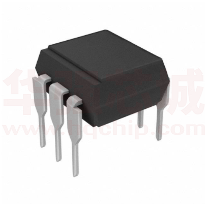
VO4154, VO4156
www.vishay.com
Vishay Semiconductors
Optocoupler, Phototriac Output, Zero Crossing,
High dV/dt, Low Input Current
FEATURES
A 1
6 MT2
• High static dV/dt 5 kV/μs
C 2
5 NC
• High input sensitivity IFT = 1.6 mA, 2 mA, and
3 mA
ZCC*
NC 3
• 300 mA on-state current
4 MT1
• Zero voltage crossing detector
*Zero crossing circuit
i179030_4
• 400 V and 600 V blocking voltage
V
D E
21842-1
• Isolation rated voltage 4420 VRMS
DESCRIPTION
• Material categorization: for definitions of compliance
please see www.vishay.com/doc?99912
The VO4154 and VO4156 consists of a GaAs IRLED
optically coupled to a photosensitive zero crossing TRIAC
packaged in a DIP-6 package.
APPLICATIONS
• Solid-state relays
High input sensitivity is achieved by using an emitter
follower phototransistor and a cascaded SCR predriver
resulting in an LED trigger current of 1.6 mA for bin D, 2 mA
for bin H, and 3 mA for bin M.
• Industrial controls
• Office equipment
• Consumer appliances
The new phototriac zero crossing family uses a proprietary
dV/dt clamp resulting in a static dV/dt of greater than
5 kV/μs.
AGENCY APPROVALS
• UL1577, file no. E52744, double protection
The VO4154 and VO4156 isolates low-voltage logic from
120 VAC, 240 VAC, and 380 VAC lines to control resistive,
inductive, or capacitive loads including motors, solenoids,
high current thyristors or TRIAC and relays.
• cUL - file no. E52744, equivalent to CSA bulletin 5A
• DIN EN 60747-5-5 (VDE 0884-5), available with option 1
ORDERING INFORMATION
V
O
4
1
5
#
X
-
PART NUMBER
X
0
0
#
PACKAGE OPTION
DIP-6
Option 6
7.62 mm
10.16 mm
Option 7
Option 9
T
TAPE
AND
REEL
> 0.7 mm
VDRM 400
AGENCY
CERTIFIED/PACKAGE
UL, cUL
> 0.1 mm
VDRM 600
TRIGGER CURRENT, IFT (mA)
1.6
2
3
1.6
2
3
VO4154D
VO4154H
VO4154M
VO4156D
VO4156H
VO4156M
DIP-6, 400 mil, option 6
VO4154D-X006
VO4154H-X006
VO4154M-X006
VO4156D-X006
VO4156H-X006
VO4156M-X006
SMD-6, option 7
VO4154D-X007T VO4154H-X007T VO4154M-X007T
DIP-6
UL, cUL, VDE
VO4156D-X007T VO4156H-X007T (1) VO4156M-X007T
1.6
2
3
1.6
2
3
DIP-6, 400 mil, option 6
-
-
-
-
VO4156H-X016
-
SMD-6, option 7
-
-
-
VO4156D-X017T
-
-
Note
• Also available in tubes, do not put “T” to the end
Rev. 1.8, 23-Oct-2018
Document Number: 84797
1
For technical questions, contact: optocoupleranswers@vishay.com
THIS DOCUMENT IS SUBJECT TO CHANGE WITHOUT NOTICE. THE PRODUCTS DESCRIBED HEREIN AND THIS DOCUMENT
ARE SUBJECT TO SPECIFIC DISCLAIMERS, SET FORTH AT www.vishay.com/doc?91000
�VO4154, VO4156
www.vishay.com
Vishay Semiconductors
ABSOLUTE MAXIMUM RATINGS (Tamb = 25 °C, unless otherwise specified)
PARAMETER
TEST CONDITION
PART
SYMBOL
VALUE
UNIT
INPUT
Reverse voltage
VR
6
V
Forward current
IF
60
mA
Surge current
IFSM
2.5
A
Power dissipation
Pdiss
100
mW
1.33
mW/°C
Derate from 25 °C
OUTPUT
Peak off-state voltage
RMS on-state current
Total power dissipation
VO4154D/H/M
VDRM
400
V
VO4156D/H/M
VDRM
600
V
ITM
300
mA
Pdiss
500
mW
6.6
mW/°C
Derate from 25 °C
COUPLER
Storage temperature range
Tstg
-55 to +150
°C
Ambient temperature range
Tamb
-55 to +100
°C
Tsld
260
°C
Max. ≤ 10 s dip soldering
≥ 0.5 mm from case bottom
Soldering temperature
Note
• Stresses in excess of the absolute maximum ratings can cause permanent damage to the device. Functional operation of the device is not
implied at these or any other conditions in excess of those given in the operational sections of this document. Exposure to absolute
maximum ratings for extended periods of the time can adversely affect reliability
350
IL - Load Current (mA)
300
250
IF = 3 mA to 10 mA
200
150
100
50
0
-40
19623
-20
0
20
40
60
80
100
Tamb - Temperature (°C)
Fig. 1 - Recommended Operating Condition
Rev. 1.8, 23-Oct-2018
Document Number: 84797
2
For technical questions, contact: optocoupleranswers@vishay.com
THIS DOCUMENT IS SUBJECT TO CHANGE WITHOUT NOTICE. THE PRODUCTS DESCRIBED HEREIN AND THIS DOCUMENT
ARE SUBJECT TO SPECIFIC DISCLAIMERS, SET FORTH AT www.vishay.com/doc?91000
�VO4154, VO4156
www.vishay.com
Vishay Semiconductors
THERMAL CHARACTERISTICS
PARAMETER
SYMBOL
VALUE
UNIT
LED power dissipation
Pdiss
100
mW
Output power dissipation
Pdiss
500
mW
Maximum LED junction temperature
Tjmax.
125
°C
Maximum output die junction temperature
Tjmax.
125
°C
Thermal resistance, junction emitter to board
θJEB
150
°C/W
Thermal resistance, junction emitter to case
θJEC
139
°C/W
Thermal resistance, junction detector to board
θJDB
78
°C/W
TA
θCA
Package
TC
θEC
θDC
θDE
TJD
TJE
θDB
θEB
TB
Thermal resistance, junction detector to case
θJDC
103
°C/W
Thermal resistance, junction emitter to
junction detector
θJED
496
°C/W
Thermal resistance, case to ambient
θCA
θBA
19996
3563
TA
°C/W
Note
• The thermal characteristics table above were measured at 25 °C and the thermal model is represented in the thermal network below. Each
resistance value given in this model can be used to calculate the temperatures at each node for a given operating condition. The thermal
resistance from board to ambient will be dependent on the type of PCB, layout and thickness of copper traces. For a detailed explanation
of the thermal model, please reference Vishay's Thermal Characteristics of Optocouplers application note
ELECTRICAL CHARACTERISTICS (Tamb = 25 °C, unless otherwise specified)
PARAMETER
TEST CONDITION
PART
SYMBOL
MIN.
TYP.
MAX.
UNIT
INPUT
Forward voltage
IF = 10 mA
VF
-
1.2
1.4
V
Reverse current
VR = 6 V
IR
-
0.1
10
μA
VF = 0 V, f = 1 MHz
CI
-
25
-
pF
VO4154D/H/M
VDRM
400
-
-
V
VO4156D/H/M
VDRM
600
-
-
V
VD = VDRM, IF = 0 A
IDRM
-
-
100
μA
On-state voltage
IT = 300 mA
VTM
-
-
3
V
On-state current
PF = 1, VT(RMS) = 1.7 V
ITM
-
-
300
mA
IF = 2 mA, VDRM
IDINH
-
-
200
μA
IH
-
-
500
μA
IF = rated IFT
VIH
-
-
20
V
VD = 0.67 VDRM, TJ = 25 °C
dV/dtcr
5000
-
-
V/μs
dV/dtcr
8
-
-
A/μs
Input capacitance
OUTPUT
Repetitive peak off-state voltage
Off-state current
Off-state current in inhibit state
IDRM = 100 μA
Holding current
Zero cross inhibit voltage
Critical rate of rise of off-state
voltage
Critical rate of rise of on-state
COUPLER
LED trigger current,
current required to latch output
VD = 3 V
Common mode coupling
capacitance
Capacitance (input to output)
f = 1 MHz, VIO = 0 V
VO4154D
IFT
-
-
1.6
mA
VO4154H
IFT
-
-
2
mA
VO4154M
IFT
-
-
3
mA
VO4156D
IFT
-
-
1.6
mA
VO4156H
IFT
-
-
2
mA
VO4156M
IFT
-
-
3
mA
CCM
-
0.01
-
pF
CIO
-
0.8
-
pF
Note
• Minimum and maximum values were tested requirements. Typical values are characteristics of the device and are the result of engineering
evaluations. Typical values are for information only and are not part of the testing requirements
Rev. 1.8, 23-Oct-2018
Document Number: 84797
3
For technical questions, contact: optocoupleranswers@vishay.com
THIS DOCUMENT IS SUBJECT TO CHANGE WITHOUT NOTICE. THE PRODUCTS DESCRIBED HEREIN AND THIS DOCUMENT
ARE SUBJECT TO SPECIFIC DISCLAIMERS, SET FORTH AT www.vishay.com/doc?91000
�VO4154, VO4156
www.vishay.com
Vishay Semiconductors
SAFETY AND INSULATION RATINGS
PARAMETER
TEST CONDITION
Climatic classification
SYMBOL
According to IEC 68 part 1
VALUE
UNIT
55 / 100 / 21
Comparative tracking index
CTI
175
VISO
4420
Maximum transient isolation voltage
VIOTM
8000
Vpeak
Maximum repetitive peak isolation voltage
VIORM
890
Vpeak
VIO = 500 V, Tamb = 25 °C
RIO
≥ 1012
Ω
VIO = 500 V, Tamb = 100 °C
RIO
≥ 1011
Ω
Output safety power
PSO
500
mW
Input safety current
ISI
250
mA
Safety temperature
TS
175
°C
≥7
mm
≥7
mm
≥ 0.4
mm
Maximum rated withstanding isolation voltage
t = 1 min
Isolation resistance
Creepage distance
Clearance distance
Insulation thickness
DTI
Pollution degree (DIN VDE 0109)
VRMS
2
Note
• As per IEC 60747-5-5, § 7.4.3.8.2, this optocoupler is suitable for “safe electrical insulation” only within the safety ratings. Compliance with
the safety ratings shall be ensured by means of protective circuits.
TYPICAL CHARACTERISTICS (Tamb = 25 °C, unless otherwise specified)
10 000
IDRM - Leakage Current (nA)
1.5
VF (V)
1.3
1.1
0 °C
25 °C
50 °C
0.9
1000
100
IRDM at 630 V
10
0.7
0.1
1
IF (mA)
19660
1
100
10
0
20008
Fig. 2 - Diode Forward Voltage vs. Forward Current
38
36
34
IR = 10 µA
32
- 60 - 40 - 20
0
20
40
60
ITM - On-State Current (mA)
VR (V)
60
80
100
1000
40
100
0 °C
10
Temperature (ºC)
25 °C
85 °C
1
1.0
80 100
Fig. 3 - Diode Reverse Voltage vs. Temperature
Rev. 1.8, 23-Oct-2018
40
Fig. 4 - Leakage Current vs. Ambient Temperature
42
19662
20
TA - Ambient Temperature (°C)
19685
1.5
IF = 2 mA
2.0
2.5
3.0
3.5
VTM - On-State Voltage (V)
Fig. 5 - On-State Current vs. On-State Voltage
Document Number: 84797
4
For technical questions, contact: optocoupleranswers@vishay.com
THIS DOCUMENT IS SUBJECT TO CHANGE WITHOUT NOTICE. THE PRODUCTS DESCRIBED HEREIN AND THIS DOCUMENT
ARE SUBJECT TO SPECIFIC DISCLAIMERS, SET FORTH AT www.vishay.com/doc?91000
�VO4154, VO4156
www.vishay.com
Vishay Semiconductors
1.4
Normalized IH
at 25 °C
85 °C
4500
1.2
4000
25 °C
3500
Normalized IH
Output Leakage current (nA)
5000
0 °C
3000
2500
2000
1500
1.0
0.8
0.6
0.4
1000
0.2
500
0
0
200
400
600
Voltage (V)
20009
-60 -40 -20
20
1.0
0.8
0.6
0.4
Normalized IFT
at 25 ºC
0.2
IFT - Trigger Current (mA)
22
1.6
1.2
20
40
60
80 100
Fig. 9 - Normalized Holding Current vs. Temperature
1.8
1.4
0
Temperature (ºC)
20011
Fig. 6 - Output Off Current (Leakage) vs. Voltage
Normalized IFT
0.0
800
18
16
14
12
85 ºC
10
100 ºC
8
6
4
-40 ºC
2
25 ºC
0
0.0
-60 -40 -20
0
20
40
60
19666
10
80 100
Temperature (ºC)
20012
Fig. 7 - Normalized Trigger Input Current vs. Temperature
20
30
40
50
60
70
Trigger Pulse Width (µs)
Fig. 10 - IFT vs. LED Pulse Width
3.5
3.0
IFT - (mA)
2.5
2.0
1.5
1.0
0.5
0
10
100
1000
Turn-On Time (µs)
20010
Fig. 8 - IFT (mA) vs. Turn-On Time (μs)
Rev. 1.8, 23-Oct-2018
Document Number: 84797
5
For technical questions, contact: optocoupleranswers@vishay.com
THIS DOCUMENT IS SUBJECT TO CHANGE WITHOUT NOTICE. THE PRODUCTS DESCRIBED HEREIN AND THIS DOCUMENT
ARE SUBJECT TO SPECIFIC DISCLAIMERS, SET FORTH AT www.vishay.com/doc?91000
�VO4154, VO4156
www.vishay.com
Vishay Semiconductors
PACKAGE DIMENSIONS in millimeters
3
2
1
4
5
6
Pin one ID
6.30
6.50
ISO method A
8.50
8.70
7.62 typ.
1.22
1.32
1 min.
3.30
3.81
4° typ.
18°
3.30
3.81
0.84 typ.
0.46
0.51
3° to 9°
0.20
0.30
0.84 typ.
7.62 to 8.81
2.54 typ.
i178014
Option 6
Option 7
Option 8
Option 9
7.62 typ.
7.62 typ.
7.62 typ.
10.3 max.
7.62 typ.
3.5 ± 0.3
0.7 min.
0.25 ± 0.1
4.3 ± 0.3
3.5 ± 0.3
0.1 ± 0.1
3.6 ± 0.3
0.1 min.
8 min.
2.55 ± 0.25
9.27 min.
0.6 min.
10.3 max.
0.6 min.
12.1 max.
8 min.
10.16 typ.
0.76
2.54
R 0.25
0.76
2.54
R 0.25
1.78
20802-50
8 min.
11.05
1.52
0.76
2.54
R 0.25
1.78
8 min.
11.05
1.52
1.78
8 min.
11.05
1.52
PACKAGE MARKING (example)
VO4154
X017
V YWW H 68
Notes
• Only options 1, 7, and 8 are reflected in the package marking
• The VDE Logo is only marked on option 1 parts
• Tape and reel suffix (T) is not part of the package marking
Rev. 1.8, 23-Oct-2018
Document Number: 84797
6
For technical questions, contact: optocoupleranswers@vishay.com
THIS DOCUMENT IS SUBJECT TO CHANGE WITHOUT NOTICE. THE PRODUCTS DESCRIBED HEREIN AND THIS DOCUMENT
ARE SUBJECT TO SPECIFIC DISCLAIMERS, SET FORTH AT www.vishay.com/doc?91000
�Legal Disclaimer Notice
www.vishay.com
Vishay
Disclaimer
ALL PRODUCT, PRODUCT SPECIFICATIONS AND DATA ARE SUBJECT TO CHANGE WITHOUT NOTICE TO IMPROVE
RELIABILITY, FUNCTION OR DESIGN OR OTHERWISE.
Vishay Intertechnology, Inc., its affiliates, agents, and employees, and all persons acting on its or their behalf (collectively,
“Vishay”), disclaim any and all liability for any errors, inaccuracies or incompleteness contained in any datasheet or in any other
disclosure relating to any product.
Vishay makes no warranty, representation or guarantee regarding the suitability of the products for any particular purpose or
the continuing production of any product. To the maximum extent permitted by applicable law, Vishay disclaims (i) any and all
liability arising out of the application or use of any product, (ii) any and all liability, including without limitation special,
consequential or incidental damages, and (iii) any and all implied warranties, including warranties of fitness for particular
purpose, non-infringement and merchantability.
Statements regarding the suitability of products for certain types of applications are based on Vishay’s knowledge of
typical requirements that are often placed on Vishay products in generic applications. Such statements are not binding
statements about the suitability of products for a particular application. It is the customer’s responsibility to validate that a
particular product with the properties described in the product specification is suitable for use in a particular application.
Parameters provided in datasheets and / or specifications may vary in different applications and performance may vary over
time. All operating parameters, including typical parameters, must be validated for each customer application by the customer’s
technical experts. Product specifications do not expand or otherwise modify Vishay’s terms and conditions of purchase,
including but not limited to the warranty expressed therein.
Except as expressly indicated in writing, Vishay products are not designed for use in medical, life-saving, or life-sustaining
applications or for any other application in which the failure of the Vishay product could result in personal injury or death.
Customers using or selling Vishay products not expressly indicated for use in such applications do so at their own risk.
Please contact authorized Vishay personnel to obtain written terms and conditions regarding products designed for
such applications.
No license, express or implied, by estoppel or otherwise, to any intellectual property rights is granted by this document
or by any conduct of Vishay. Product names and markings noted herein may be trademarks of their respective owners.
© 2017 VISHAY INTERTECHNOLOGY, INC. ALL RIGHTS RESERVED
Revision: 08-Feb-17
1
Document Number: 91000
�Mouser Electronics
Authorized Distributor
Click to View Pricing, Inventory, Delivery & Lifecycle Information:
Vishay:
VO4154D VO4154D-X006 VO4154D-X007T VO4154H VO4154H-X006 VO4154H-X007T VO4154M VO4154MX006 VO4154M-X007T VO4156D VO4156D-X006 VO4156D-X007T VO4156H VO4156H-X006 VO4156H-X007T
VO4156M VO4156M-X006 VO4156M-X007T VO4156H-X016 VO4156H-X007
�