VOD223T
www.vishay.com
Vishay Semiconductors
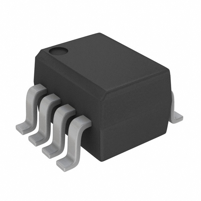
Optocoupler, Photodarlington Output, Dual Channel,
SOIC-8 Package
FEATURES
A 1
8C
C2
7 E
• High current transfer ratio at IF = 1 mA,
500 % minimum
A 3
6C
• Isolation test voltage, 4000 VRMS
C4
5 E
• Material categorization:
for definitions of compliance please see
www.vishay.com/doc?99912
i179074
DESCRIPTION
AGENCY APPROVALS
The VOD233T is a high current transfer ratio (CTR)
optocoupler. It has a gallium arsenide infrared LED emitter
and silicon NPN photodarlington transistor detector.
• UL1577, file no. E52744 system code Y
This device has CTRs tested at an LED current of 1 mA. This
low drive current permits easy interfacing from CMOS to
LSTTL or TTL.
• DIN EN 60747-5-5 (VDE 0884) available with option 1
• cUL - file no. E52744, equivalent to CSA bulletin 5A
ORDERING INFORMATION
SOIC-8
V
O
D
2
2
3
T
PART NUMBER
6.1 mm
AGENCY CERTIFIED/PACKAGE
CTR (%)
≥ 500
UL, cUL, VDE
SOIC-8
VOD223T
ABSOLUTE MAXIMUM RATINGS (Tamb = 25 °C, unless otherwise specified)
PARAMETER
TEST CONDITION
SYMBOL
VALUE
UNIT
VR
6
V
1 μs, 300 pps
IFM
3
A
IF
30
mA
Pdiss
45
mW
0.4
mW/°C
INPUT
Peak reverse voltage
Peak pulsed current
Continuous forward current per channel
Power dissipation
Derate linearly from 25 °C
OUTPUT
Collector emitter breakdown voltage
BVCEO
30
V
Emitter collector breakdown voltage
BVECO
5
V
75
mW
3.1
mW/°C
VISO
4000
VRMS
Ptot
250
mW
2
mW/°C
Storage temperature
Tstg
-40 to +150
°C
Operating temperature
Tamb
-40 to +100
°C
Soldering temperature (1)
Tsld
260
°C
Power dissipation per channel
Derate linearly from 25 °C
COUPLER
Isolation test voltage
Total package dissipation
(2 LEDs and 2 detectors, 2 channels)
Pdiss
t=1s
Derate linearly from 25 °C
Notes
• Stresses in excess of the absolute maximum ratings can cause permanent damage to the device. Functional operation of the device is not
implied at these or any other conditions in excess of those given in the operational sections of this document. Exposure to absolute
maximum ratings for extended periods of the time can adversely affect reliability.
(1) Refer to reflow profile for soldering conditions for surface mounted devices (SOP/SOIC).
Rev. 1.3, 10-Dec-14
Document Number: 81959
1
For technical questions, contact: optocoupleranswers@vishay.com
THIS DOCUMENT IS SUBJECT TO CHANGE WITHOUT NOTICE. THE PRODUCTS DESCRIBED HEREIN AND THIS DOCUMENT
ARE SUBJECT TO SPECIFIC DISCLAIMERS, SET FORTH AT www.vishay.com/doc?91000
�VOD223T
www.vishay.com
Vishay Semiconductors
ELECTRICAL CHARACTERISTICS (Tamb = 25 °C, unless otherwise specified)
PARAMETER
TEST CONDITION
SYMBOL
Forward voltage
IF = 10 mA
VF
Reverse current
VR = 6 V
VF = 0 V, f = 1 MHz
MIN.
TYP.
MAX.
UNIT
1.3
V
IR
0.1
100
μA
CO
25
INPUT
Capacitance
pF
OUTPUT
Collector emitter breakdown voltage
IC = 100 μA
BVCEO
30
V
Emitter collector breakdown voltage
IC = 10 μA
BVECO
5
V
VCE = 5 V, IF = 0 A
ICEO
VCE = 5 V
CCE
IF = 1 mA, ICE = 0.5 mA
VCEsat
Collector emitter leakage current
Collector emitter capacitance
Saturation voltage, collector emitter
50
3.4
nA
pF
1
V
COUPLER
Capacitance (input to output)
0.5
CIO
pF
Note
• Minimum and maximum values are testing requirements. Typical values are characteristics of the device and are the result of engineering
evaluation. Typical values are for information only and are not part of the testing requirements.
CURRENT TRANSFER RATIO (Tamb = 25 °C, unless otherwise specified)
PARAMETER
TEST CONDITION
SYMBOL
MIN.
IC/IF
IF = 1 mA, VCE = 5 V
CTRDC
500
TYP.
MAX.
UNIT
%
SWITCHING CHARACTERISTICS (Tamb = 25 °C, unless otherwise specified)
PARAMETER
TEST CONDITION
SYMBOL
MIN.
Turn-on time
VCC = 10 V, RL = 100 Ω, IF = 5 mA
ton
15
TYP.
MAX.
UNIT
μs
Turn-off time
VCC = 10 V, RL = 100 Ω, IF = 5 mA
toff
30
μs
VCC = 10 V
IF
f = 10 kHz,
DF = 50 %
trise
VO
10 %
RL
VO
toff
50 %
IF = 5 mA
90 %
iild223t_09
ton
tfall
Fig. 1 - Switching Test Circuit
Rev. 1.3, 10-Dec-14
Document Number: 81959
2
For technical questions, contact: optocoupleranswers@vishay.com
THIS DOCUMENT IS SUBJECT TO CHANGE WITHOUT NOTICE. THE PRODUCTS DESCRIBED HEREIN AND THIS DOCUMENT
ARE SUBJECT TO SPECIFIC DISCLAIMERS, SET FORTH AT www.vishay.com/doc?91000
�VOD223T
www.vishay.com
Vishay Semiconductors
SAFETY AND INSULATION RATINGS
PARAMETER
TEST CONDITION
Climatic classification
SYMBOL
MIN.
according to IEC 68 part 1
TYP.
MAX.
UNIT
40/100/21
Polution degree
2
Comparative tracking index
CTI
175
VISO
4000
VRMS
Peak transient overvoltage
VIOTM
6000
V
Peak insulation voltage
VIORM
560
V
Safety rating - power output
PSO
Resistance (input to output)
RIO
Apparent charge method a
qpd
C
Apparent charge method b
qpd
C
Isolation test voltage
1s
399
350
mW
100
GW
Safety rating - input current
ISI
150
mA
Safety rating - temperature
TSI
165
°C
External creepage distance
4
mm
Internal creepage distance
4
mm
4
mm
0.2
mm
External clearance distance
Insulation thickness
Note
• As per IEC 60747-5-2, §7.4.3.8.1, this optocoupler is suitable for “safe electrical insulation” only within the safety ratings. Compliance with
the safety ratings shall be ensured by means of prodective circuits.
TYPICAL CHARACTERISTICS (Tamb = 25 °C, unless otherwise specified)
10 000
1.3
If(pk) - Peak LED Current (mA)
VF - Forward Voltage (V)
1.4
TA = - 55 °C
1.2
TA = 25 °C
1.1
1.0
0.9
TA = 100 °C
0.8
0.7
0.1
iild223t_01
1
10
100
IF - Forward Current (mA)
Fig. 2 - Forward Voltage vs. Forward Current
Rev. 1.3, 10-Dec-14
τ
Duty Factor
0.005
1000 0.01
0.02
0.05
0.1
0.2
0.5
100
t
DF= τ/t
10
10-6 10-5 10-4
iild223t_02
10-3 10-2 10-1 100
101
t - LED Pulse Duration (s)
Fig. 3 - Peak LED Current vs. Duty Factor, t
Document Number: 81959
3
For technical questions, contact: optocoupleranswers@vishay.com
THIS DOCUMENT IS SUBJECT TO CHANGE WITHOUT NOTICE. THE PRODUCTS DESCRIBED HEREIN AND THIS DOCUMENT
ARE SUBJECT TO SPECIFIC DISCLAIMERS, SET FORTH AT www.vishay.com/doc?91000
�VOD223T
www.vishay.com
Vishay Semiconductors
1000
TA = - 20 °C
TA = 25 °C
TA = 50 °C
TA = 70 °C
10
ICE - Collector Current (mA)
Normalized CTRce
100
1
Normalized to:
IF = 1 mA, VCE = 5 V
TA = 25 °C
0.1
VCE = 5 V
10
1
0.1
1
10
0.1
100
I F - LED Current (mA)
iil221at_04
iil221at_07
Fig. 4 - Normalized CTRCE vs. LED Current
CTRce - Current Transfer Ratio (%)
100
Tamb = - 20 °C
Tamb = 25 °C
Tamb = 50 °C
Tamb = 70 °C
10
1
100
IF - LED Current (mA)
Fig. 6 - Collector Current vs. LED Current
2000
Tamb = - 20 °C
Tamb = 25 °C
Tamb = 50 °C
Tamb = 70 °C
1500
VCE = 5 V
1000
500
0
0.1
1
10
100
IF - LED Current (mA)
iild223t_04
Fig. 5 - CTR vs. LED Current
PACKAGE DIMENSIONS in millimeters
6.35 max.
4.60 typ.
5.80 ± 0.15
3.90 ± 0.15
0.41 typ.
1.27 nom.
7
6
5
0.35 min.
4.45 min.
Leads coplanarity
0.1 max.
R0.13
0.91
1.27
0.36
8
0.15 ± 0.05
3.15 ± 0.20
0.20 ± 0.05
6.27 max.
4.32
6.60
PIN ONE I.D.
1
Rev. 1.3, 10-Dec-14
2
3
1.14
4
Document Number: 81959
4
For technical questions, contact: optocoupleranswers@vishay.com
THIS DOCUMENT IS SUBJECT TO CHANGE WITHOUT NOTICE. THE PRODUCTS DESCRIBED HEREIN AND THIS DOCUMENT
ARE SUBJECT TO SPECIFIC DISCLAIMERS, SET FORTH AT www.vishay.com/doc?91000
�VOD223T
www.vishay.com
Vishay Semiconductors
PACKAGE MARKING (example)
223
V YWW Y 68
TAPE AND REEL PACKAGING
Dimensions in millimeters
ESD sticker
4 ± 0.1
1.5 min.
Pin 1 and
top of component
2 ± 0.05
10 pitch cumulative
tolerance on tape
± 0.2
0.3 max.
Tape slot
in core
1.75 ± 0.1
Top
cover
tape
6.6
330
(13")
7.5 ± 0.05
3.8
16.0 ± 0.3
6.35
13.3
8.0
Regular, special
or bar code label
0.1 max.
18004-1
Center lines
of cavity
Embossment
1.5
Direction of feed
17999
Fig. 7 - Tape and Reel Shipping Medium
(EIA-481, revision A, and IEC 60286), 2000 units per reel
Rev. 1.3, 10-Dec-14
Fig. 8 - Tape Dimensions, 2000 Parts per Reel
Document Number: 81959
5
For technical questions, contact: optocoupleranswers@vishay.com
THIS DOCUMENT IS SUBJECT TO CHANGE WITHOUT NOTICE. THE PRODUCTS DESCRIBED HEREIN AND THIS DOCUMENT
ARE SUBJECT TO SPECIFIC DISCLAIMERS, SET FORTH AT www.vishay.com/doc?91000
�Legal Disclaimer Notice
www.vishay.com
Vishay
Disclaimer
ALL PRODUCT, PRODUCT SPECIFICATIONS AND DATA ARE SUBJECT TO CHANGE WITHOUT NOTICE TO IMPROVE
RELIABILITY, FUNCTION OR DESIGN OR OTHERWISE.
Vishay Intertechnology, Inc., its affiliates, agents, and employees, and all persons acting on its or their behalf (collectively,
“Vishay”), disclaim any and all liability for any errors, inaccuracies or incompleteness contained in any datasheet or in any other
disclosure relating to any product.
Vishay makes no warranty, representation or guarantee regarding the suitability of the products for any particular purpose or
the continuing production of any product. To the maximum extent permitted by applicable law, Vishay disclaims (i) any and all
liability arising out of the application or use of any product, (ii) any and all liability, including without limitation special,
consequential or incidental damages, and (iii) any and all implied warranties, including warranties of fitness for particular
purpose, non-infringement and merchantability.
Statements regarding the suitability of products for certain types of applications are based on Vishay’s knowledge of
typical requirements that are often placed on Vishay products in generic applications. Such statements are not binding
statements about the suitability of products for a particular application. It is the customer’s responsibility to validate that a
particular product with the properties described in the product specification is suitable for use in a particular application.
Parameters provided in datasheets and / or specifications may vary in different applications and performance may vary over
time. All operating parameters, including typical parameters, must be validated for each customer application by the customer’s
technical experts. Product specifications do not expand or otherwise modify Vishay’s terms and conditions of purchase,
including but not limited to the warranty expressed therein.
Except as expressly indicated in writing, Vishay products are not designed for use in medical, life-saving, or life-sustaining
applications or for any other application in which the failure of the Vishay product could result in personal injury or death.
Customers using or selling Vishay products not expressly indicated for use in such applications do so at their own risk.
Please contact authorized Vishay personnel to obtain written terms and conditions regarding products designed for
such applications.
No license, express or implied, by estoppel or otherwise, to any intellectual property rights is granted by this document
or by any conduct of Vishay. Product names and markings noted herein may be trademarks of their respective owners.
© 2017 VISHAY INTERTECHNOLOGY, INC. ALL RIGHTS RESERVED
Revision: 08-Feb-17
1
Document Number: 91000
�