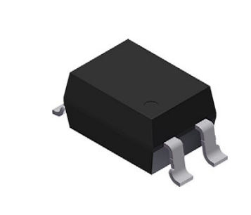
VOR1142B4
www.vishay.com
Vishay Semiconductors
1 Form A Solid-State Relay
FEATURES
• Isolation test voltage 5300 VRMS
• Typical RON 22 Ω
4 S1
A 1
• Load voltage 400 V
• Load current 140 mA
C 2
3
• Clean bounce free switching
S2
• Current limit protection
• Low power consumption
• Wide temperature range
• Material categorization: for definitions of compliance
please see www.vishay.com/doc?99912
DESCRIPTION
The VOR1142 is a 400 V single channel normally open
optically isolated solid-state relay (SPST - 1 form A). Based
on hybrid architecture which allows fast switching times
with a wide operating ambient temperature range. A high
efficient GaAlAs IRED enables low forward current on the
input side. On the output side high performance MOSFET
switches provide a low RON and can switch both DC and AC
signals.
APPLICATIONS
• General telecom switching
• Metering
• Security equipment
• Instrumentation
• Industrial controls
• Battery management systems
• Automatic test equipment
AGENCY APPROVALS
• UL1577, file no. E52744
• DIN EN 60747-5-5 (VDE 0884-5)
ORDERING INFORMATION
V
O
R
1
1
4
2
B
4
#
SMD-4
PART NUMBER
PACKAGE
PACKAGE
CONFIGURATION
UL, VDE
SMD-4, tape and reel
VOR1142B4T
SMD-4, tube
VOR1142B4
Rev. 1.0, 09-Jun-16
Document Number: 84299
1
For technical questions, contact: optocoupleranswers@vishay.com
THIS DOCUMENT IS SUBJECT TO CHANGE WITHOUT NOTICE. THE PRODUCTS DESCRIBED HEREIN AND THIS DOCUMENT
ARE SUBJECT TO SPECIFIC DISCLAIMERS, SET FORTH AT www.vishay.com/doc?91000
�VOR1142B4
www.vishay.com
Vishay Semiconductors
ABSOLUTE MAXIMUM RATINGS (Tamb = 25 °C, unless otherwise specified)
PARAMETER
CONDITION
SYMBOL
VALUE
UNIT
IRED continuous forward current
IF
50
mA
IRED reverse voltage
VR
5
V
Pdiss
80
mW
DC or peak AC load voltage
VL
400
V
Continuous DC load current at 25 °C,
bidirectional
IL
140
mA
Pdiss
550
mW
Tamb
-40 to +100
°C
Tstg
-40 to +150
°C
Tsld
260
°C
INPUT
Input power dissipation
OUTPUT
SSR output power dissipation
SSR
Ambient temperature range
Storage temperature range
Soldering temperature
t = 10 s max.
Note
• Stresses in excess of the absolute maximum ratings can cause permanent damage to the device. Functional operation of the device is not
implied at these or any other conditions in excess of those given in the operational sections of this document. Exposure to absolute
maximum ratings for extended periods of the time can adversely affect reliability.
ELECTRICAL CHARACTERISTICS (Tamb = 25 °C, unless otherwise specified)
PARAMETER
TEST CONDITION
SYMBOL
MIN.
TYP.
MAX.
UNIT
IRED forward current, switch turn-on
IL = 100 mA, t = 10 ms
IFon
-
0.25
2
mA
IRED forward current, switch turn-off
VL = ± 350 V, IL < 1 μA
IFoff
0.05
0.15
-
mA
IRED forward voltage
IF = 10 mA
VF
-
1.36
1.5
V
IRED reverse current
VR = 5 V
IR
-
-
10
μA
INPUT
OUTPUT
On-resistance, AC/DC: pin 3 (±) to 4 (±)
Off-resistance
Off-state leakage current
Output capacitance pin 3 to 4
Current limit AC/DC
IF = 5 mA, IL = 50 mA
RON
-
22
27
Ω
IF = 0 mA, VL = ± 100 V
ROFF
1
5000
-
GΩ
IF = 0 mA, VL = ± 100 V
IO
-
很抱歉,暂时无法提供与“VOR1142B4”相匹配的价格&库存,您可以联系我们找货
免费人工找货- 国内价格 香港价格
- 1+24.250871+3.14166
- 10+21.5782810+2.79543
- 25+20.6103725+2.67004
- 50+19.9063250+2.57883
- 100+19.22458100+2.49052
- 300+18.19049300+2.35655
- 500+17.72825500+2.29667
- 1000+17.119511000+2.21781
- 5000+15.784055000+2.04480
- 国内价格
- 50+11.66038
- 100+11.42711
- 200+11.19904
- 国内价格
- 5+12.20502
- 15+11.93634
- 25+11.68433