VS-10RIA Series
www.vishay.com
Vishay Semiconductors
Medium Power Phase Control Thyristors
(Stud Version), 10 A
FEATURES
• Improved glass passivation for high reliability
and exceptional stability at high temperature
• High dIF/dt and dV/dt capabilities
• Standard package
• Low thermal resistance
• Metric threads version available
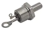
TO-48 (TO-208AA)
• Types up to 1200 V VDRM/VRRM
PRIMARY CHARACTERISTICS
• Designed and qualified for industrial and consumer level
IT(AV)
10 A
VDRM/VRRM
100 V, 200 V, 400 V, 600 V, 800 V,
1000 V, 1200 V
• Material categorization: for definitions of compliance
please see www.vishay.com/doc?99912
VTM
1.75 V
TYPICAL APPLICATIONS
IGT
60 mA
• Medium power switching
TJ
-65 °C to +125 °C
• Phase control applications
Package
TO-48 (TO-208AA)
Circuit configuration
Single SCR
MAJOR RATINGS AND CHARACTERISTICS
PARAMETER
TEST CONDITIONS
IT(AV)
TC
IT(RMS)
ITSM
I2t
UNITS
10
A
85
°C
25
A
50 Hz
225
60 Hz
240
50 Hz
255
60 Hz
233
VDRM/VRRM
tq
VALUES
Typical
TJ
A
A2s
100 to 1200
V
110
μs
-65 to +125
°C
ELECTRICAL SPECIFICATIONS
VOLTAGE RATINGS
TYPE
NUMBER
VS-10RIA
VOLTAGE
CODE
VDRM/VRRM, MAXIMUM REPETITIVE PEAK
AND OFF-STATE VOLTAGE (1)
V
VRSM, MAXIMUM NON-REPETITIVE
PEAK VOLTAGE (2)
V
IDRM/IRRM MAXIMUM
AT TJ = TJ MAXIMUM
mA
10
100
150
20
20
200
300
40
400
500
60
600
700
80
800
900
100
1000
1100
120
1200
1300
10
Notes
(1) Units may be broken over non-repetitively in the off-state direction without damage, if dI/dt does not exceed 20 A/μs
(2) For voltage pulses with t 5 ms
p
Revision: 21-Sep-17
Document Number: 93689
1
For technical questions within your region: DiodesAmericas@vishay.com, DiodesAsia@vishay.com, DiodesEurope@vishay.com
THIS DOCUMENT IS SUBJECT TO CHANGE WITHOUT NOTICE. THE PRODUCTS DESCRIBED HEREIN AND THIS DOCUMENT
ARE SUBJECT TO SPECIFIC DISCLAIMERS, SET FORTH AT www.vishay.com/doc?91000
�VS-10RIA Series
www.vishay.com
Vishay Semiconductors
ABSOLUTE MAXIMUM RATINGS
PARAMETER
SYMBOL
Maximum average on-state current
at case temperature
Maximum RMS on-state current
IT(AV)
TEST CONDITIONS
180° conduction, half sine wave
IT(RMS)
t = 10 ms
Maximum peak, one-cycle
non-repetitive surge current
ITSM
t = 8.3 ms
t = 10 ms
t = 8.3 ms
t = 10 ms
Maximum
I2t
I2t
for fusing
t = 8.3 ms
t = 10 ms
t = 8.3 ms
Maximum I2t for fusing
I2t
No voltage
reapplied
UNITS
10
A
85
°C
25
A
225
No voltage
reapplied
100 % VRRM
reapplied
VALUES
240
190
Sinusoidal half wave,
initial TJ =TJ maximum
100 % VRRM
reapplied
t = 0.1 to 10 ms, no voltage reapplied
A
200
255
233
180
A2s
165
2550
Low level value of threshold voltage
VT(TO)1
(16.7 % x x IT(AV) < I < x IT(AV)), TJ = TJ maximum
1.10
High level value of threshold voltage
VT(TO)2
(I > x IT(AV)), TJ = TJ maximum
1.39
Low level value of
on-state slope resistance
rt1
(16.7 % x x IT(AV) < I < x IT(AV)), TJ = TJ maximum
24.3
High level value of
on-state slope resistance
rt2
(I > x IT(AV)), TJ = TJ maximum
16.7
Ipk = 32 A, TJ = 25 °C, tp = 10 ms sine pulse
1.75
A2s
V
m
Maximum on-state voltage
VTM
Maximum holding current
IH
Typical latching current
IL
TJ = 25 °C, anode supply 12 V resistive load
130
200
V
mA
SWITCHING
PARAMETER
SYMBOL
VDRM 600 V
Maximum rate of rise VDRM 800 V
of turned-on current VDRM 1000 V
Typical reverse recovery time
Typical turn-off time
VALUES
UNITS
200
dIF/dt
VDRM 1600 V
Typical turn-on time
TEST CONDITIONS
TJ = TJ maximum, VDM = Rated VDRM
Gate pulse = 20 V, 15 , tp = 6 μs, tr = 0.1 μs maximum
ITM = (2 x rated dI/dt) A
180
160
A/μs
150
tgt
TJ = 25 °C, at rated VDRM/VRRM, TJ = 125 °C
trr
TJ = TJ maximum,
ITM = IT(AV), tp > 200 μs, dIF/dt = - 10 A/μs
tq
TJ = TJ maximum, ITM = IT(AV), tp > 200 μs, VR = 100 V,
dIF/dt = - 10 A/μs, dV/dt = 20 V/μs linear to 67 % VDRM,
gate bias 0 V to 100 W
0.9
4
μs
110
Note
• tq = 10 μs up to 600 V, tq = 30 μs up to 1600 V available on special request
BLOCKING
PARAMETER
Maximum critical rate of rise
of off-state voltage
SYMBOL
dV/dt
TEST CONDITIONS
VALUES
TJ = TJ maximum linear to 100 % rated VDRM
100
TJ = TJ maximum linear to 67 % rated VDRM
300 (1)
UNITS
V/μs
Note
(1) Available with: dV/dt = 1000 V/μs, to complete code add S90 i.e. 10RIA120S90
Revision: 21-Sep-17
Document Number: 93689
2
For technical questions within your region: DiodesAmericas@vishay.com, DiodesAsia@vishay.com, DiodesEurope@vishay.com
THIS DOCUMENT IS SUBJECT TO CHANGE WITHOUT NOTICE. THE PRODUCTS DESCRIBED HEREIN AND THIS DOCUMENT
ARE SUBJECT TO SPECIFIC DISCLAIMERS, SET FORTH AT www.vishay.com/doc?91000
�VS-10RIA Series
www.vishay.com
Vishay Semiconductors
TRIGGERING
PARAMETER
SYMBOL
Maximum peak gate power
PGM
Maximum average gate power
PG(AV)
TEST CONDITIONS
VALUES
8.0
TJ = TJ maximum
2.0
UNITS
W
Maximum peak positive gate current
IGM
TJ = TJ maximum
1.5
A
Maximum peak negative gate voltage
-VGM
TJ = TJ maximum
10
V
TJ = -65 °C
90
DC gate current required to trigger
IGT
TJ = 25 °C
TJ = -65 °C
DC gate voltage required to trigger
VGT
60
Maximum required gate trigger
current/voltage are the lowest value
which will trigger all units 6 V anode
to cathode applied
TJ = 125 °C
TJ = 25 °C
3.0
2.0
TJ = 125 °C
DC gate current not to trigger
IGD
DC gate voltage not to trigger
VGD
mA
35
V
1.0
TJ = TJ maximum, VDRM = Rated value
TJ = TJ maximum,
VDRM = Rated value
Maximum gate current/voltage not
to trigger is the maximum value
which will not trigger any unit with
rated VDRM anode to cathode
applied
2.0
mA
0.2
V
THERMAL AND MECHANICAL SPECIFICATIONS
PARAMETER
SYMBOL
Maximum operating junction and
storage temperature range
TEST CONDITIONS
TJ, TStg
VALUES
UNITS
-65 to +125
°C
Maximum thermal resistance,
junction to case
RthJC
DC operation
1.85
Maximum thermal resistance,
case to heat sink
RthCS
Mounting surface, smooth, flat and greased
0.35
K/W
Lubricated threads
(Non-lubricated threads)
Mounting torque
Approximate weight
Case style
See dimensions - link at the end of datasheet
TO NUT
TO DEVICE
20 (27.5)
25
lbf in
0.23 (0.32)
0.29
kgf · m
2.3 (3.1)
2.8
N·m
14
g
0.49
oz.
TO-48 (TO-208AA)
RthJC CONDUCTION
CONDUCTION ANGLE
SINUSOIDAL CONDUCTION
RECTANGULAR CONDUCTION
180°
0.44
0.32
120°
0.53
0.56
90°
0.68
0.75
60°
1.01
1.05
30°
1.71
1.73
TEST CONDITIONS
UNITS
TJ = TJ maximum
K/W
Note
• The table above shows the increment of thermal resistance RthJC when devices operate at different conduction angles than DC
Revision: 21-Sep-17
Document Number: 93689
3
For technical questions within your region: DiodesAmericas@vishay.com, DiodesAsia@vishay.com, DiodesEurope@vishay.com
THIS DOCUMENT IS SUBJECT TO CHANGE WITHOUT NOTICE. THE PRODUCTS DESCRIBED HEREIN AND THIS DOCUMENT
ARE SUBJECT TO SPECIFIC DISCLAIMERS, SET FORTH AT www.vishay.com/doc?91000
�VS-10RIA Series
130
Vishay Semiconductors
10RIA Series
RthJC (DC) = 1.85 K/W
120
110
100
90
Conduction Angle
80
30°
60°
70
90°
120°
60
180°
50
40
0
2
4
6
8
10
12 14
130
Maximum Allowable Case Temperature (°C)
Maximum Allowable Case Temperature (°C)
www.vishay.com
10RIA Series
RthJC (DC) = 1.85 K/W
120
110
100
90
Conduction Period
80
30°
60°
70
90°
120°
60
180°
50
DC
40
0
16 18
Fig. 1 - Current Ratings Characteristics
10
15
20
25
30
Fig. 2 - Current Ratings Characteristics
35
1
W
K/
3K
/W
ta
el
-D
4K
/W
RMS Limit
5K
/W
7K
/W
15
Conduction Angle
10
10RIA Series
TJ = 125°C
5
R
20
K/
W
=
25
2
A
180°
120°
90°
60°
30°
30
S
R th
Maximum Average On-state Power Loss (W)
5
Average On-state Current (A)
Average On-state Current (A)
10 K
/W
0
0
2
4
6
8
10 12
14 16
Average On-state Current (A)
0
18
25
50
75
100
125
Maximum Allowable Ambient Temperature (°C)
45
DC
180°
120°
90°
60°
30°
40
35
30
R
SA
th
Maximum Average On-state Power Loss (W)
Fig. 3 - On-State Power Loss Characteristics
25
20
=
1
2K
/W
3K
/W
4K
/W
RMS Limit
15
Conduction Period
10
5K
/W
7 K/W
10RIA Series
TJ = 125°C
10 K/W
5
K/
W
-D
el
ta
R
0
0
5
10
15
20
25
Average On-state Current (A)
0
30
25
50
75
100
125
Maximum Allowable Ambient Temperature (°C)
Fig. 4 - On-State Power Loss Characteristics
Revision: 21-Sep-17
Document Number: 93689
4
For technical questions within your region: DiodesAmericas@vishay.com, DiodesAsia@vishay.com, DiodesEurope@vishay.com
THIS DOCUMENT IS SUBJECT TO CHANGE WITHOUT NOTICE. THE PRODUCTS DESCRIBED HEREIN AND THIS DOCUMENT
ARE SUBJECT TO SPECIFIC DISCLAIMERS, SET FORTH AT www.vishay.com/doc?91000
�VS-10RIA Series
www.vishay.com
240
200
At Any Rated Load Condition And With
Rated V RRMApplied Following Surge.
Initial T J= 125°C
@ 60 Hz 0.0083 s
@ 50 Hz 0.0100 s
190
180
170
Peak Half Sine Wave On-state Current (A)
Peak Half Sine Wave On-state Current (A)
Vishay Semiconductors
160
150
140
130
120
110
10RIA Series
100
90
1
10
Maximum Non Repetitive Surge Current
Versus Pulse Train Duration. Control
Of Conduction May Not Be Maintained.
Initial TJ = 125°C
No Voltage Reapplied
Rated V RRMReapplied
220
200
180
160
140
120
100
10RIA Series
80
0.01
100
Fig. 5 - Maximum Non-Repetitive Surge Current
Instantaneous On-state Current (A)
0.1
1
Pulse Train Duration (s)
Number Of Equal Amplitude Half Cycle Current Pulses (N)
Fig. 6 - Maximum Non-Repetitive Surge Current
1000
100
TJ = 25°C
TJ = 125°C
10
10RIA Series
1
0.5
1
1.5
2
2.5
3
3.5
4
Instantaneous On-state Voltage (V)
Transient Thermal Impedance ZthJC (K/W)
Fig. 7 - Forward Voltage Drop Characteristics
10
Steady State Value
R thJC = 1.85 K/W
(DC Operation)
1
10RIA Series
0.1
0.001
0.01
0.1
1
10
Square Wave Pulse Duration (s)
Fig. 8 - Thermal Impedance ZthJC Characteristics
Revision: 21-Sep-17
Document Number: 93689
5
For technical questions within your region: DiodesAmericas@vishay.com, DiodesAsia@vishay.com, DiodesEurope@vishay.com
THIS DOCUMENT IS SUBJECT TO CHANGE WITHOUT NOTICE. THE PRODUCTS DESCRIBED HEREIN AND THIS DOCUMENT
ARE SUBJECT TO SPECIFIC DISCLAIMERS, SET FORTH AT www.vishay.com/doc?91000
�VS-10RIA Series
www.vishay.com
Vishay Semiconductors
Rectangular gate pulse
a) Recommended load line for
rated di/dt : 10V, 20ohms
tr = 6 µs
b) Recommended load line for