VS-1KAB-E Series
www.vishay.com
Vishay Semiconductors
Single Phase Rectifier Bridge, 1.2 A
FEATURES
• Ease of assembly, installation, inventory
• High surge rating
• Compact
• Material categorization: for definitions of compliance
please see www.vishay.com/doc?99912
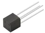
DESCRIPTION
D-38
A 1.2 A diode bridge rectifier assembly designed for new
circuits and for replacement service. For printed circuit
board applications.
PRIMARY CHARACTERISTICS
IO
1.2 A
VRRM
100 V to 1000 V
Package
D-38
Circuit configuration
Single phase bridge
MAJOR RATINGS AND CHARACTERISTICS
SYMBOL
CHARACTERISTICS
IO
IFSM
I2t
VALUES
UNITS
1.2
A
50 Hz
50
60 Hz
52
50 Hz
17.7
60 Hz
16.1
VRRM
TJ
A
A2s
100 to 1000
V
-55 to 150
°C
ELECTRICAL SPECIFICATIONS
VOLTAGE RATINGS
CROSS REFERENCE
PART
NUMBER
DIN CODE
VS-1KAB05E
VRRM, VRSM
(V)
VRMS
(RECOMMENDED)
(V)
MAXIMUM
LOAD CAPACITANCE
(μF) (1)
MINIMUM
SOURCE RESISTANCE
() (1)
50
20
7000
0.5
VS-1KAB10E
B40C1000
100
40
5000
0.5
VS-1KAB20E
B80C1000
200
80
3300
0.8
VS-1KAB40E
B125C1000
400
125
1600
1.5
VS-1KAB60E
B250C1000
600
250
1200
2.6
VS-1KAB80E
B380C1000
800
380
800
3.0
VS-1KAB100E
B500C1000
1000
500
600
5.0
Note
(1) See figure 3
Revision: 14-Sep-17
Document Number: 93559
1
For technical questions within your region: DiodesAmericas@vishay.com, DiodesAsia@vishay.com, DiodesEurope@vishay.com
THIS DOCUMENT IS SUBJECT TO CHANGE WITHOUT NOTICE. THE PRODUCTS DESCRIBED HEREIN AND THIS DOCUMENT
ARE SUBJECT TO SPECIFIC DISCLAIMERS, SET FORTH AT www.vishay.com/doc?91000
�VS-1KAB-E Series
www.vishay.com
Vishay Semiconductors
FORWARD CONDUCTION
PARAMETER
SYMBOL
Maximum DC output current
IO
Maximum peak one cycle,
non-repetitive surge current
TEST CONDITIONS
1.2
TA = 45 °C, capacitive load
1.0
50 Hz half cycle sine wave
or 6 ms rectangular pulse
IFSM
60 Hz half cycle sine wave
or 5 ms rectangular pulse
t = 10 ms
Maximum I2t capability for fusing
t = 8.3 ms
I2t
VALUES
TA = 45 °C, resistive or inductive load
t = 10 ms
t = 8.3 ms
Following any rated load
condition, and with rated
VRRM applied following surge
UNITS
A
50
A
52
Rated VRRM applied
following surge, initial
TJ = 150 °C
12.5
VRRM = 0 following surge,
initial TJ = 150 °C
17.7
11.3
A2s
16.1
Maximum I2t capability for fusing
I2t (1)
t = 0.1 to 10 ms, VRRM following surge = 0
177
A2s
Maximum peak forward voltage per leg
VFM
IO = 1.2 A (1.88 Apk)
1.1
V
TJ = 25 °C, at rated VRRM
10
TJ = 150 °C, at rated VRRM
500
Typical peak reverse current per leg
IRM
Operating frequency range
f
μA
40 to 2000
Hz
Note
(1) I2t for time t = I2t x t
x
x
THERMAL AND MECHANICAL SPECIFICATIONS
PARAMETER
Operating junction and storage temperature range
SYMBOL
VALUES
UNITS
TJ, TStg
-40 to 150
°C
3
g
0.1
oz.
Approximate weight
Maximum Peak Output Current (A)
Average Output Current (A)
1.4
1.2
Resistive, inductive load
1.0
0.8
0.6
Capacitive load
0.4
0.2
0
0
20
40
60
80
100
120
140
160
60
Following any rated load
condition and with rated
VRRM applied following surge
50
40
30
20
10
0
10-2
10-1
1
10
Maximum Allowable Ambient Temperature (°C)
Equal Amplitude Pulse Train Duration (s)
Fig. 1 - Average (DC) Output Current vs.
Maximum Allowable Ambient Temperature
Fig. 2 - Maximum Non-Repetitive Surge Current vs.
Pulse Train Duration (f = 50 Hz)
Revision: 14-Sep-17
Document Number: 93559
2
For technical questions within your region: DiodesAmericas@vishay.com, DiodesAsia@vishay.com, DiodesEurope@vishay.com
THIS DOCUMENT IS SUBJECT TO CHANGE WITHOUT NOTICE. THE PRODUCTS DESCRIBED HEREIN AND THIS DOCUMENT
ARE SUBJECT TO SPECIFIC DISCLAIMERS, SET FORTH AT www.vishay.com/doc?91000
�VS-1KAB-E Series
www.vishay.com
10
CL = 200 µF
CL = 400 µF
Average Output Current (A)
RMS Supply Voltage (V)
600
Vishay Semiconductors
500
CL = 600 µF
400
CL = 800 µF
300
CL = 1600 µF
CL = 1200 µF
200
CL = 3300 µF
CL = 5000 µF
100
CL = 7000 µF
5
Resistive, inductive load
2
Capacitive load
1
Initial TJ = 45 °C
0.5
0
0
1
2
3
4
5
6
10-1
1
10
102
103
Minimum Required Value of Source Resistance (Ω)
Switch-On Surge Duration (s)
Fig. 3 - Minimum Required Source Resistance vs.
RMS Supply Voltage and Load Capacitance
Fig. 4 - Maximum Switch-On Surge Current vs.
Surge Duration
CIRCUIT CONFIGURATION
AC
(+)
AC
(-)
LINKS TO RELATED DOCUMENTS
Dimensions
www.vishay.com/doc?95327
Revision: 14-Sep-17
Document Number: 93559
3
For technical questions within your region: DiodesAmericas@vishay.com, DiodesAsia@vishay.com, DiodesEurope@vishay.com
THIS DOCUMENT IS SUBJECT TO CHANGE WITHOUT NOTICE. THE PRODUCTS DESCRIBED HEREIN AND THIS DOCUMENT
ARE SUBJECT TO SPECIFIC DISCLAIMERS, SET FORTH AT www.vishay.com/doc?91000
�Outline Dimensions
www.vishay.com
Vishay Semiconductors
D-38
DIMENSIONS in millimeters (inches)
5.10 (0.201)
4.30 (0.169)
9.70 (0.382)
8.70 (0.343)
~
+
-
~
5.10 (0.201)
4.30 (0.169)
9.70 (0.382)
8.70 (0.343)
10.30 (0.405)
9.30 (0.366)
25.40 (1.000)
24.00 (0.945)
0.90 (0.035)
0.70 (0.028)
5.10 (0.201)
4.30 (0.169)
Document Number: 95327
1
For technical questions, contact: indmodules@vishay.com
THIS DOCUMENT IS SUBJECT TO CHANGE WITHOUT NOTICE. THE PRODUCTS DESCRIBED HEREIN AND THIS DOCUMENT
ARE SUBJECT TO SPECIFIC DISCLAIMERS, SET FORTH AT www.vishay.com/doc?91000
Revision: 13-Jul-2020
�Legal Disclaimer Notice
www.vishay.com
Vishay
Disclaimer
ALL PRODUCT, PRODUCT SPECIFICATIONS AND DATA ARE SUBJECT TO CHANGE WITHOUT NOTICE TO IMPROVE
RELIABILITY, FUNCTION OR DESIGN OR OTHERWISE.
Vishay Intertechnology, Inc., its affiliates, agents, and employees, and all persons acting on its or their behalf (collectively,
“Vishay”), disclaim any and all liability for any errors, inaccuracies or incompleteness contained in any datasheet or in any other
disclosure relating to any product.
Vishay makes no warranty, representation or guarantee regarding the suitability of the products for any particular purpose or
the continuing production of any product. To the maximum extent permitted by applicable law, Vishay disclaims (i) any and all
liability arising out of the application or use of any product, (ii) any and all liability, including without limitation special,
consequential or incidental damages, and (iii) any and all implied warranties, including warranties of fitness for particular
purpose, non-infringement and merchantability.
Statements regarding the suitability of products for certain types of applications are based on Vishay's knowledge of typical
requirements that are often placed on Vishay products in generic applications. Such statements are not binding statements
about the suitability of products for a particular application. It is the customer's responsibility to validate that a particular product
with the properties described in the product specification is suitable for use in a particular application. Parameters provided in
datasheets and / or specifications may vary in different applications and performance may vary over time. All operating
parameters, including typical parameters, must be validated for each customer application by the customer's technical experts.
Product specifications do not expand or otherwise modify Vishay's terms and conditions of purchase, including but not limited
to the warranty expressed therein.
Hyperlinks included in this datasheet may direct users to third-party websites. These links are provided as a convenience and
for informational purposes only. Inclusion of these hyperlinks does not constitute an endorsement or an approval by Vishay of
any of the products, services or opinions of the corporation, organization or individual associated with the third-party website.
Vishay disclaims any and all liability and bears no responsibility for the accuracy, legality or content of the third-party website
or for that of subsequent links.
Except as expressly indicated in writing, Vishay products are not designed for use in medical, life-saving, or life-sustaining
applications or for any other application in which the failure of the Vishay product could result in personal injury or death.
Customers using or selling Vishay products not expressly indicated for use in such applications do so at their own risk. Please
contact authorized Vishay personnel to obtain written terms and conditions regarding products designed for such applications.
No license, express or implied, by estoppel or otherwise, to any intellectual property rights is granted by this document or by
any conduct of Vishay. Product names and markings noted herein may be trademarks of their respective owners.
© 2023 VISHAY INTERTECHNOLOGY, INC. ALL RIGHTS RESERVED
Revision: 01-Jan-2023
1
Document Number: 91000
�